Method of verifying photomask data based on models of etch and lithography processes

a technology of etching and lithography, applied in the field of optical lithography, can solve the problems that the opc algorithm has not always met this goal, and the verification has been performed using an optical model

Inactive Publication Date: 2010-12-07
CADENCE DESIGN SYST INC
View PDF12 Cites 60 Cited by
  • Summary
  • Abstract
  • Description
  • Claims
  • Application Information

AI Technical Summary

Problems solved by technology

In the prior art, OPC algorithms have not always met this goal.
A deficiency in the prior art is that verification has been performed using an optical model.

Method used


Image

  • Method of verifying photomask data based on models of etch and lithography processes
  • Method of verifying photomask data based on models of etch and lithography processes
  • Method of verifying photomask data based on models of etch and lithography processes

Examples


Embodiment Construction

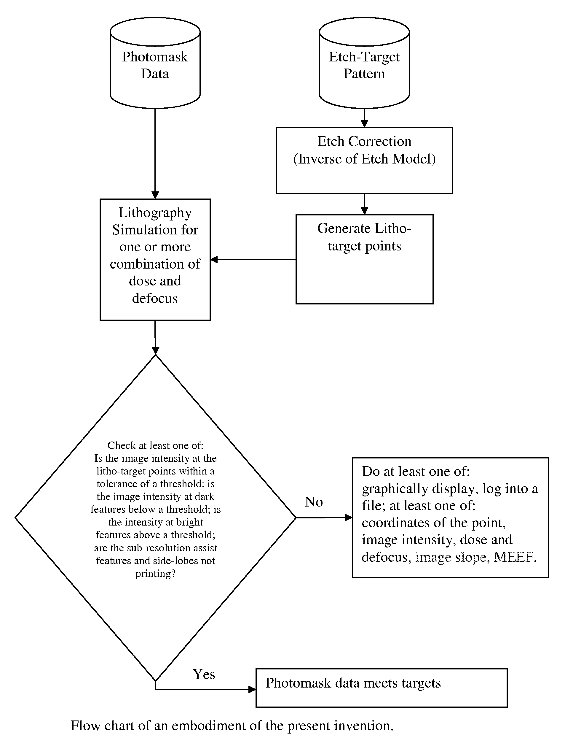
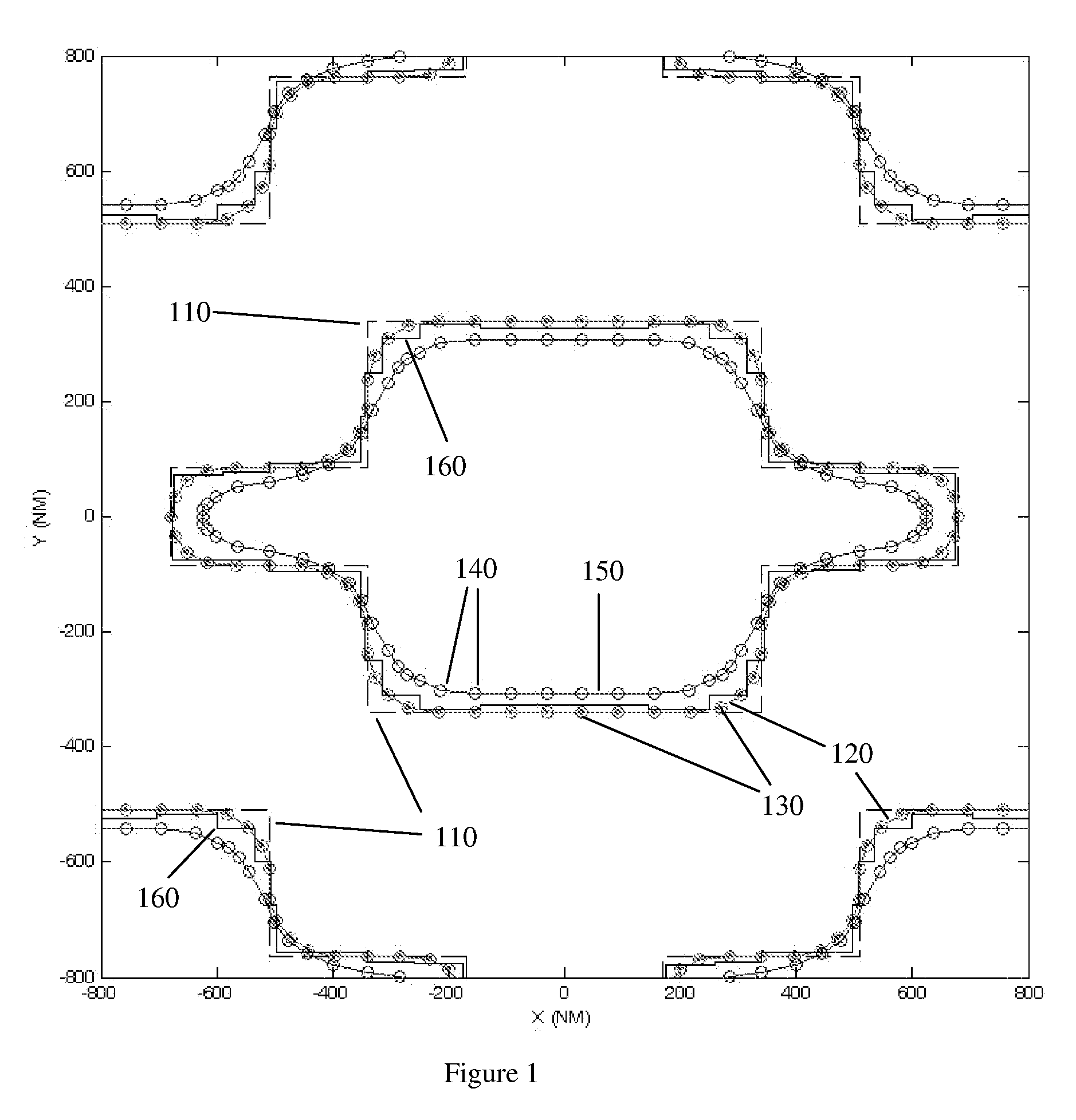
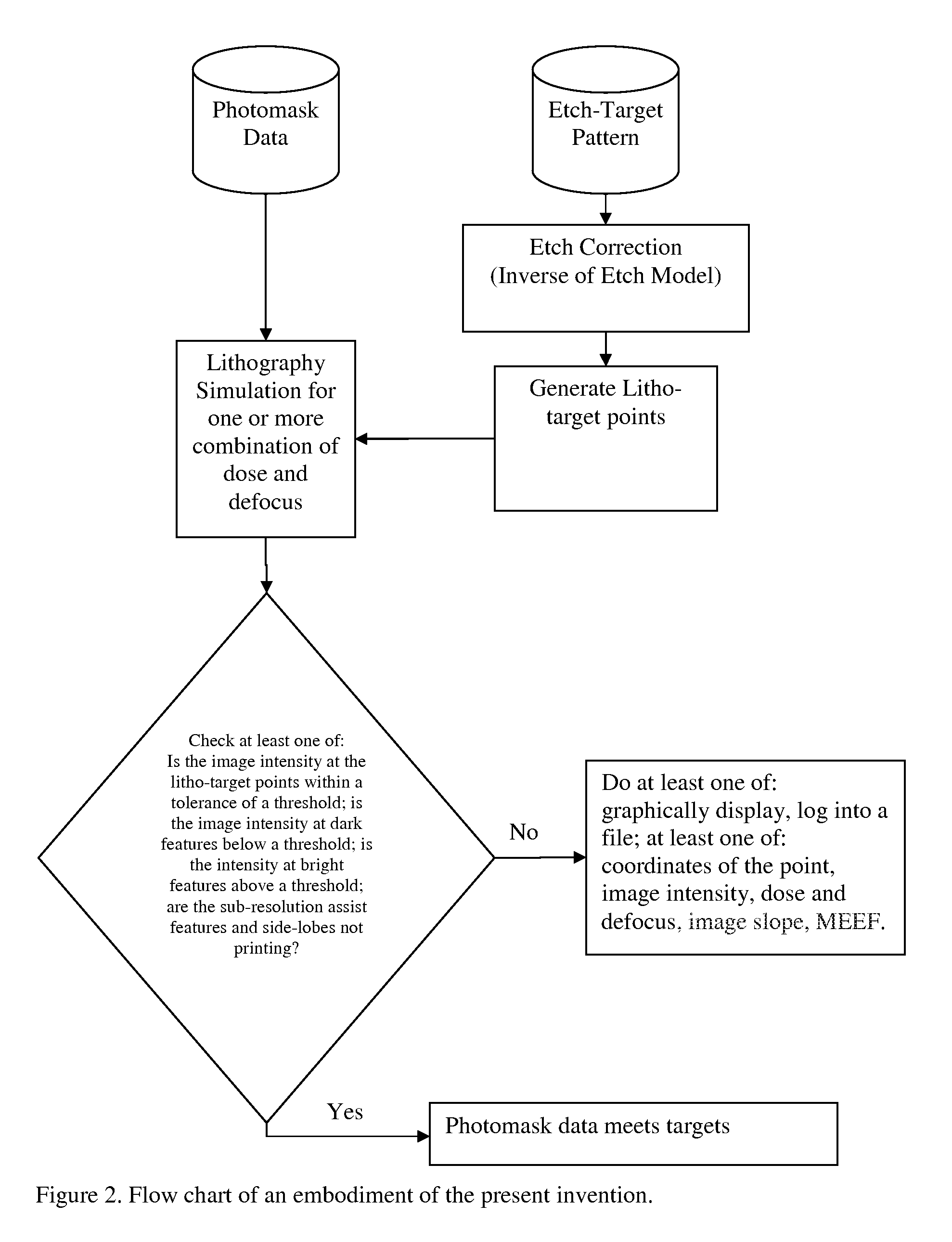
[0036]Photolithography transfers pattern(s) from one or more photomasks to a photoresist film coated on a semiconductor wafer. The pattern that is formed in photoresist acts as a mask, or a stencil, during a subsequent etching process. Critical features of integrated circuits are usually etched by so called plasma-etch or dry-etch processes. The dimensions of a feature in photoresist are different from the dimensions of the same feature, etched into a layer on the wafer. This difference between an etched dimension and the corresponding resist dimension is called: etch-bias or etch-skew. The etch-bias depends on the local details of the pattern and on the surrounding pattern density. In other words, the etch bias depends on some aspects of the pattern that is being etched. To be valid, verification has to account for the etch bias. For this purpose, we introduce the concepts of etch-target and litho-target.

[0037]Etch-target is a set of polygons or a set of curves that describe the de...


PUM


Abstract

A photomask dataset corresponding to a target-pattern is verified by simulating a resist-pattern that will be formed in a resist layer by a lithography process, simulating an etched-pattern that will be etched in a layer by a plasma process wherein said simulation comprises calculating a flux of particles impacting a feature, and determining whether the etched-pattern substantially conforms to the target-pattern.

Description

CROSS-REFERENCE TO RELATED APPLICATION[0001]This application claims benefit of U.S. Provisional Application No. 60 / 807,967 filed Jul. 21, 2006, the entire disclosure of which is incorporated herein by reference.FIELD OF THE INVENTION[0002]This invention relates to the general field of optical lithography. In particular, this invention relates to verifying that a given photomask data set will meet a set of design targets.BACKGROUND[0003]Layers of semiconductor devices are patterned using lithography and etch processes. Both of these processes distort the pattern that is being transferred from a photomask to a layer on a semiconductor wafer.[0004]The pattern to be formed on the wafer will be called the target pattern for the purposes of this application. The target pattern is produced by design steps that include considerations of circuit function, electrical parameters of devices, placement of components on an integrated circuit, routing of connections, parasitic electrical parameter...

Claims


Application Information

Patent Timeline
Patent Type & Authority Patents(United States)
IPC IPC(8): G06F17/50G06F9/45
CPCG03F1/36
Inventor YENIKAYA, BAYRAMJOSHI, DEVENDRAFORNARI, PAUL A.CARRERO, JESUS O.SEZGINER, ABDURRAHMAN
Owner CADENCE DESIGN SYST INC
Why Eureka
Try Eureka