Storage device and data output circuit

a storage device and data output technology, applied in memory adressing/allocation/relocation, instruments, program control, etc., can solve the problems of troublesome job, troublesome job, long manufacturing time, etc., and achieve the effect of simplifying the manufacturing process

Active Publication Date: 2010-12-28
MEGACHIPS
View PDF5 Cites 1 Cited by
  • Summary
  • Abstract
  • Description
  • Claims
  • Application Information

AI Technical Summary

Benefits of technology

[0011]An object of the present invention is to provide a technique for supplying a memory that simplifies the manufacturing process on the supplier side while satisfying specifications provided from the user side.

Problems solved by technology

For the supplier of the ROM using a write-type nonvolatile memory, the writing of the fixed value FXVL is a troublesome job because it lengthens the manufacturing time.
It is also a troublesome job to check the fixed value FXVL in the no-write region 203 in the test conducted prior to the shipment.

Method used


Image

  • Storage device and data output circuit
  • Storage device and data output circuit
  • Storage device and data output circuit

Examples


first preferred embodiment

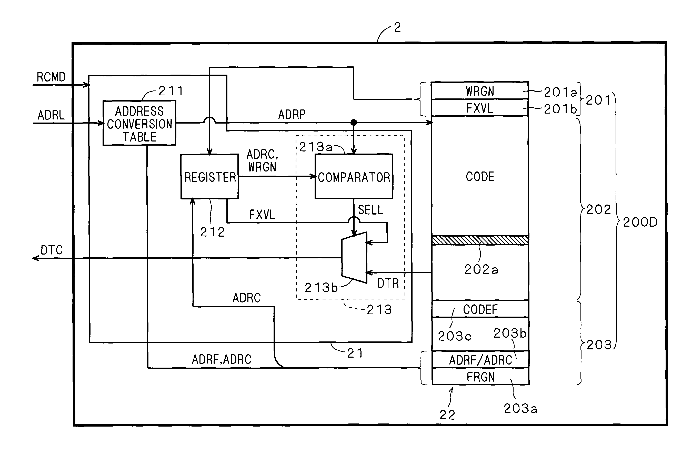
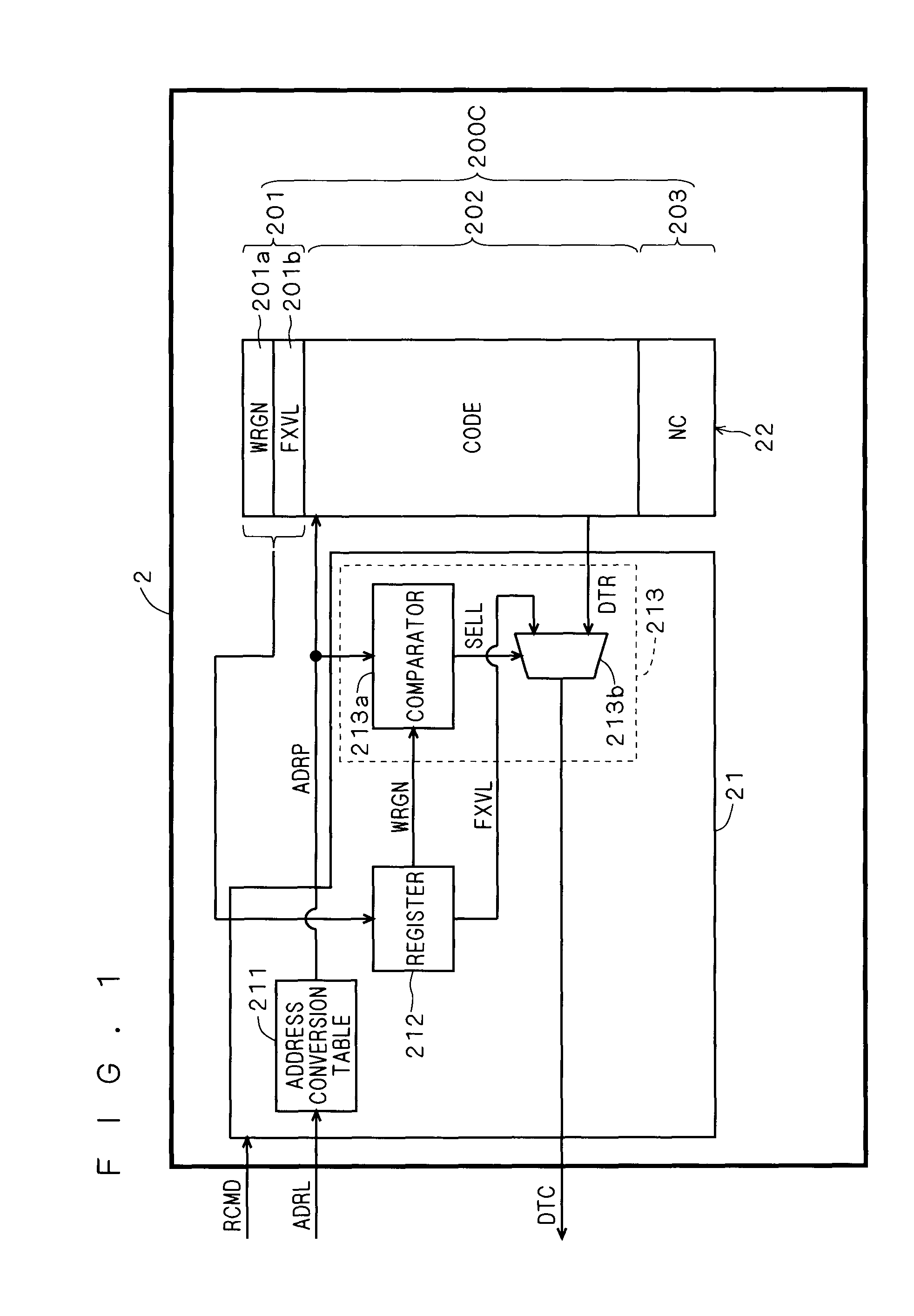
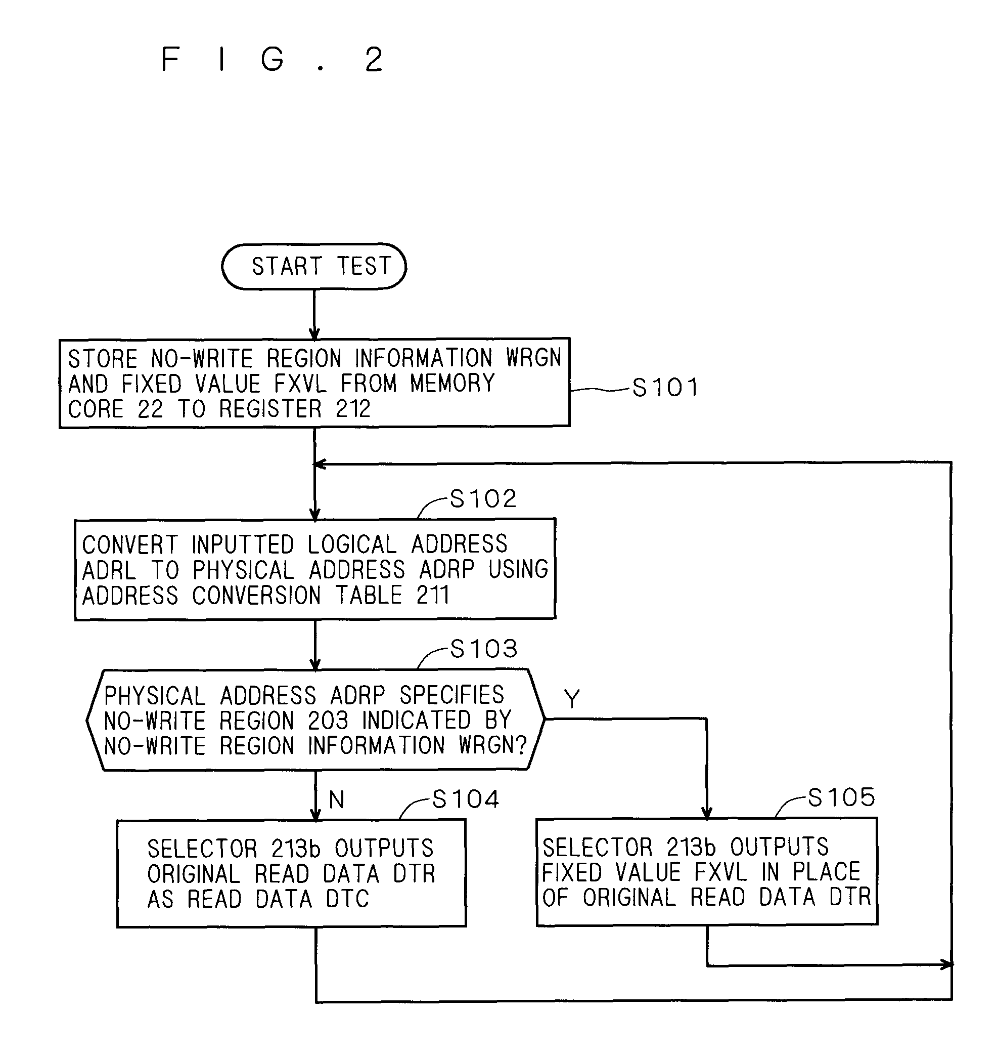
[0046]FIG. 1 is a block diagram illustrating the configuration of a ROM 2 as a storage device according to a first preferred embodiment of the present invention. The ROM 2 includes a controller 21 and a memory core 22.

[0047]The memory core 22 is indicated with an address space 200C. The address space 200C includes an information storage region 201, a code region 202, and a no-write region 203. The information storage region 201 includes a first region 201a in which no-write region information WRGN is written, and a second region 201b in which a fixed value FXVL is written. Program code CODE is written in the code region 202. It is not necessary to apply an active write operation to the no-write region 203, and unknown values NC exist there.

[0048]The no-write region information WRGN indicates the position of the no-write region 203, or specifically physical addresses in the address space 200C, and the fixed value FXVL indicates a fixed value that is intended to be written to the no-w...

second preferred embodiment

[0062]The technique described in the first preferred embodiment can be applied to provide a so-called redundancy region in the no-write region 203. This is because the ROM 2 can be regarded as storing the fixed value FXVL in the no-write region 203, irrespective of the values actually stored in the no-write region 203.

[0063]FIG. 3 is a block diagram illustrating the configuration of a ROM 2 as a storage device according to a second preferred embodiment of the present invention. The configuration adopts the block shown in the first preferred embodiment, but signals are differently sent and received in some ways.

[0064]For a first difference, the address space 200C is replaced by an address space 200D. The address space 200D includes a redundancy indication region 203a, a redundancy conversion region 203b, and a redundancy region 203c that are provided in the no-write region 203.

[0065]The redundancy indication region 203a stores redundancy indication information FRGN that indicates the...

third preferred embodiment

[0091]The specification 100 of a ROM to which program code is written is not always provided in the form as illustrated in FIG. 12. FIG. 6 is a diagram conceptually showing another example of the specification 100. This specification 100 simply specifies logical addresses and a group of data DATA to be stored at the logical addresses. FIG. 7 is a diagram conceptually illustrating the contents of the data group DATA. Program code CODE1 and a fixed value group VL1 are located at different addresses. The fixed value group VL1 is a collection of fixed values FXVL.

[0092]When the specification 100 is provided in such a form, the no-write region information WRGN indicating the position of the fixed value group VL1 and the constituent fixed values FXVL are obtained by scanning the entirety of the data group DATA.

[0093]Since the specification does not specify addresses for storing the no-write region information WRGN and fixed values FXVL, the no-write region information WRGN and fixed value...


PUM


Abstract

A memory is provided which simplifies the manufacturing process on the supplier side while satisfying specifications provided from the user side. An address space of a memory core includes an information storage region, a code region, and a no-write region. The information storage region includes a first region where no-write region information is written and a second region where a fixed value is written. Program code is written in the code region. The no-write region information indicates the position of the no-write region, and the fixed value indicates a fixed value that is intended to be written to the no-write region. The ROM selects between the fixed value and original read data that is obtained by a data selecting section directly from the memory core, and outputs the selected one as read data.

Description

BACKGROUND OF THE INVENTION[0001]1. Field of the Invention[0002]The present invention relates to a technique of reading data from a memory.[0003]2. Description of the Background Art[0004]For the supply of a ROM (Read Only Memory) in which program code is written, the specifications may specify not only the program code itself but also the data stored in the entire ROM. One of the purposes thereof is to previously avoid problems that would be caused when data is read from a memory area not intended for access by the user of the ROM.[0005]FIG. 12 is a diagram conceptually showing an example of a specification 100 of a ROM in which program code is written. Such a specification 100 often specifies not only the program code CODE but also no-write region information WRGN and a fixed value FXVL. The no-write region information WRGN indicates a region where the program code CODE should not be stored (hereinafter referred to also as a no-write region). The fixed value FXVL is fixed value dat...

Claims


Application Information

Patent Timeline
Patent Type & Authority Patents(United States)
IPC IPC(8): G06F12/00
CPCG06F12/02G11C17/14
Inventor OSHIKIRI, TAKASHI
Owner MEGACHIPS
Why Eureka
Try Eureka