Wafer transfer apparatus and substrate transfer apparatus

a substrate transfer and transfer apparatus technology, applied in the field of transfer apparatus, can solve the problems of reducing affecting the speed of the transfer apparatus, and the cleanliness of the interface space b>9/b> may tend to be degraded, so as to reduce the weight of the robot b>7/b>, the minimum rotation radius r and the link length of each link member of the robot arm can be increased

Active Publication Date: 2011-01-25
KAWASAKI HEAVY IND LTD
View PDF22 Cites 16 Cited by
  • Summary
  • Abstract
  • Description
  • Claims
  • Application Information

AI Technical Summary

Benefits of technology

[0016]Accordingly, it is an object of the present invention to provide a wafer transfer apparatus having a wafer transfer robot which can suppress scattering of dust and prevent occurrence of interference in the interior of the wafer transfer apparatus, and has a simple structure and can be readily controlled.
[0017]Another object of the present invention is to provide a substrate transfer apparatus having a substrate transfer robot which can suppress scattering of dust and prevent occurrence of interference in the interior of the substrate transfer apparatus, and has a simple structure and can be readily controlled.

Problems solved by technology

It is difficult, however, to seal the direct acting mechanism against dust to be generated in a driving portion, as compared with the case of a rotation driving mechanism.
Therefore, due to dust to be generated by the running means, cleanliness in the interface space 9 may tend to be degraded.
In addition, the running means 12 should also be of a large size in order to support the robot main body 13, thus making it difficult to downsize the robot 7 and reduce the weight thereof.
In addition, the provision of such a running means 12 leads to further increase of the production cost.
However, in the case of increasing the number of the link members of the robot arm 14, the robot structure should be complicated so much.
Additionally, the increase of the link members increases in turn redundancy of the robot, as such control of the robot arm 14 may tend to be difficult.
For example, in regard to the wafer transfer, a teaching operation for teaching transformed states of the robot arm may be further complicated.
Such problems may occur in other apparatuses than the wafer transfer apparatus.
Specifically, in the case of substrate transfer apparatuses each provided with a substrate carrying robot for carrying each substrate in the interface space which is maintained in a predetermined atmosphere, the same problems as those describe above may occur.

Method used


Image

  • Wafer transfer apparatus and substrate transfer apparatus
  • Wafer transfer apparatus and substrate transfer apparatus
  • Wafer transfer apparatus and substrate transfer apparatus

Examples


first embodiment

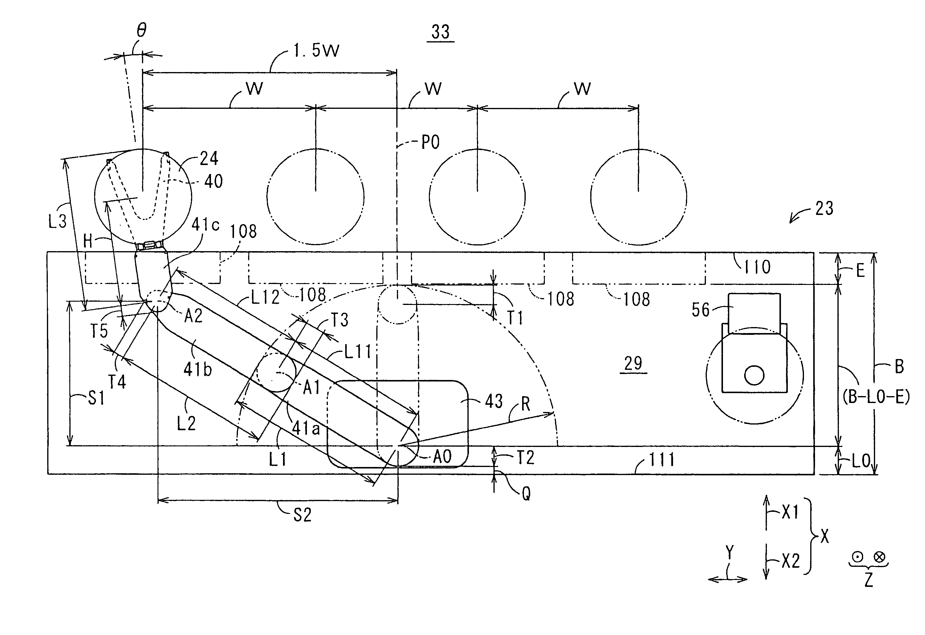
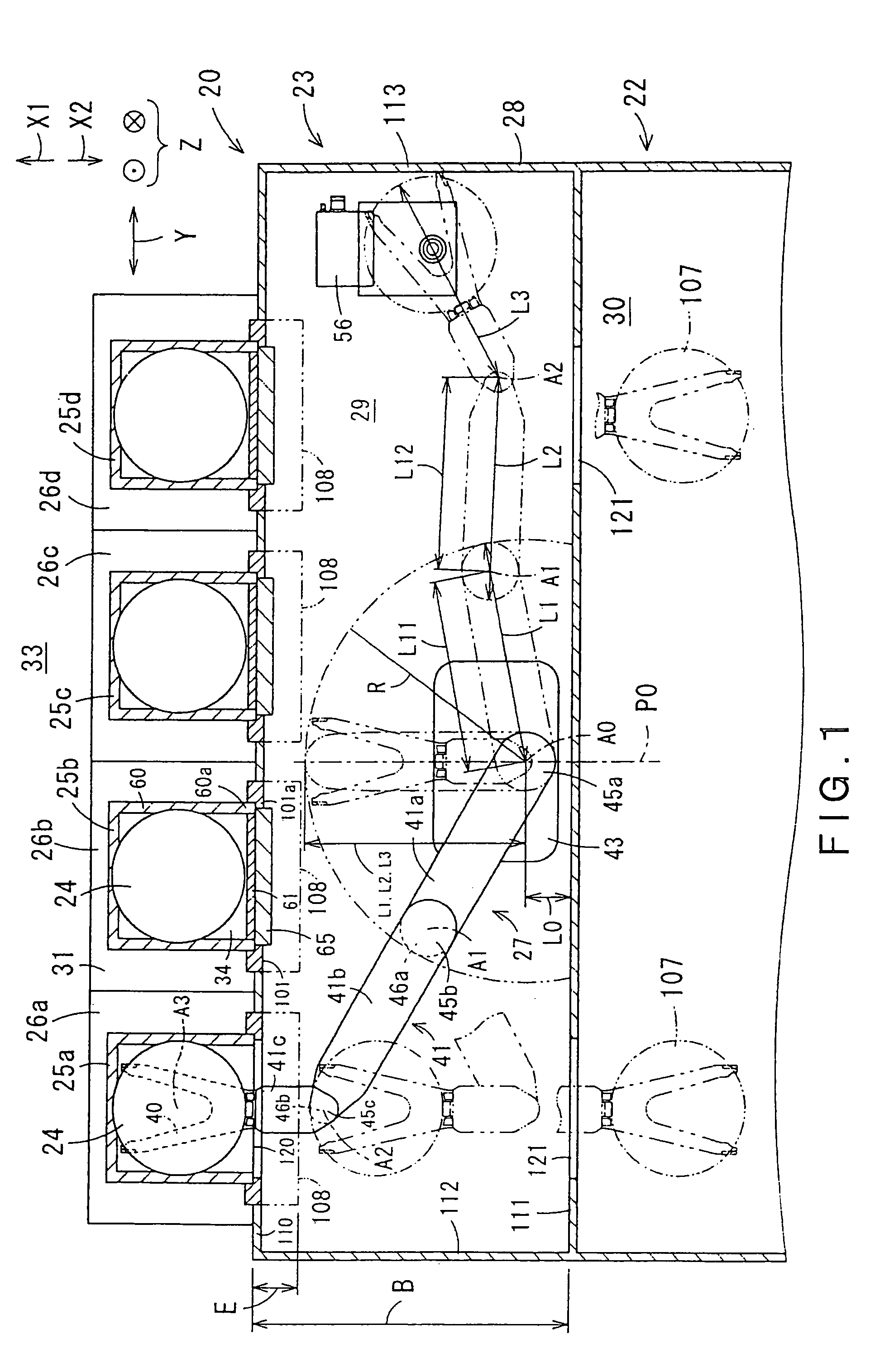
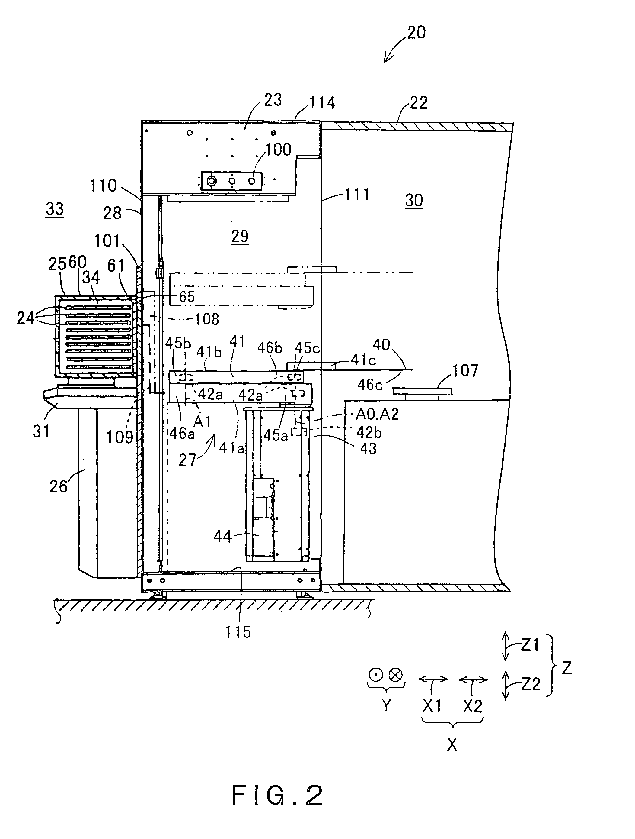
[0061]As shown in FIGS. 1 and 2, the semiconductor processing equipment 20 according to the present invention provides a predetermined process to each semiconductor wafer 24 which is a substrate to be processed. For example, as the process to be provided to the semiconductor wafer 24, various processes including heating, impurity doping, film forming, lithography, washing or flattening may be included. In addition, the semiconductor processing equipment 20 may perform other substrate processes than those described above.

[0062]The semiconductor processing equipment 20 performs the aforementioned processes in a processing space 30 filled with an atmospheric gas having adequate cleanliness. Wafers 24 are carried into the semiconductor processing equipment 20 while being contained in large numbers in a-substrate container referred to as a front opening unified pod (FOUP) 25. Each FOUP 25 is intended to serve as a mini-environmental substrate container configured to provide a clean envir...

fourth embodiment

[0157]In the fourth embodiment, it is preferred that the rear opening 121 is provided in the vicinity of the pivot axis A0 with respect to the left and right directions Y. It is also preferred that the rear opening 121 is formed to have a space extending longer than a distance between a first crossing point P1 that is one of two crossing points, at which an imaginary circle defined to make a circuit around the pivot axis A0, with its radius being the minimum rotation radius R of the robot 27, crosses the rear-face-side wall 111 and a second point P2, at which a line passing through the pivot axis A0 and extending in the forward and backward directions X crosses the rear-face-side wall 111, as such the space is shaped to include both of the first crossing point P1 and the second crossing point P2. Consequently, in the case of angularly displacing the first link member 41a about the pivot axis A0, interference of the first link member 41a with the rear-face-side wall 111 can be preven...


PUM


Abstract

A wafer transfer apparatus is provided. In a minimum transformed state where a robot arm is transformed such that a distance defined from a pivot axis to an arm portion, which is farthest in a radial direction relative to the pivot axis, is minimum, a minimum rotation radius R, is set to exceed ½ of a length B in the forward and backward directions of an interface space, the length B corresponding to a length between the front wall and the rear wall of the interface space forming portion, and is further set to be equal to or less than a subtracted value obtained by subtracting a distance L0 in the forward and backward directions from the rear wall of the interface space forming portion to the pivot axis, from the length B in the forward and backward directions of the interface space (i.e., B / 2<R≦B−L0).

Description

CROSS REFERENCE TO RELATED APPLICATIONS[0001]This application is based upon the prior Japanese Patent Application No. 2006-198771 filed on Jul. 20, 2006, the entire contents of which are incorporated herein by reference.BACKGROUND OF THE INVENTION[0002]1. Field of the Invention[0003]The present invention relates to a wafer transfer apparatus for use in semiconductor processing equipment. The present invention also relates to a substrate transfer apparatus for transferring a substrate in an interface space, which is maintained in a predetermined atmosphere, of a substrate processing equipment.[0004]2. Description of the Related Art[0005]FIG. 13 is a section showing a semiconductor processing equipment 1 of the related art, which is partly cut away. The semiconductor processing equipment 1 is configured to include a wafer processing apparatus 2 and a wafer transfer apparatus 3. The wafer transfer apparatus is an equipment front end module (EFEM). Spaces 9, 10 in the semiconductor proc...

Claims


Application Information

Patent Timeline
Patent Type & Authority Patents(United States)
IPC IPC(8): H01L21/677
CPCH01L21/67766Y10S414/139Y10S414/135Y10S414/137G05B19/41815H01L21/67742H01L21/68707G05B2219/45031
Inventor HASHIMOTO, YASUHIKO
Owner KAWASAKI HEAVY IND LTD
Why Eureka
Try Eureka