Imaging device including a plurality of lens elements and a imaging sensor

a technology of imaging sensor and lens element, which is applied in the field of imaging device, can solve the problems of large lens diameter, volume increase, and insufficiently achieved size reduction, and achieve the effect of high image resolution

Inactive Publication Date: 2011-02-01
PANASONIC CORP
View PDF15 Cites 61 Cited by
  • Summary
  • Abstract
  • Description
  • Claims
  • Application Information

AI Technical Summary

Benefits of technology

[0023]According to the present invention, a thin imaging device is provided in which a high image resolution is obtained and in which the resolution does not uniformly vary even when the shooting distance is changed. Further, according to the present invention, a lens array is provided that is suitable for this imaging device.

Problems solved by technology

Nevertheless, in the imaging devices constructed from an imaging optical system and an image sensor such as a CCD (Charge Coupled Device) sensor or a MOS (Metal Oxide Semiconductor) sensor, size reduction, especially thickness reduction, is not yet achieved satisfactorily.
A conventional optical system in which a plurality of lens elements are arranged on the optical axis has problems that the length increases in the optical axis direction and hence the volume increases, and that the lens diameter is large and hence the aberration increases.

Method used


Image

  • Imaging device including a plurality of lens elements and a imaging sensor
  • Imaging device including a plurality of lens elements and a imaging sensor
  • Imaging device including a plurality of lens elements and a imaging sensor

Examples


embodiment 1

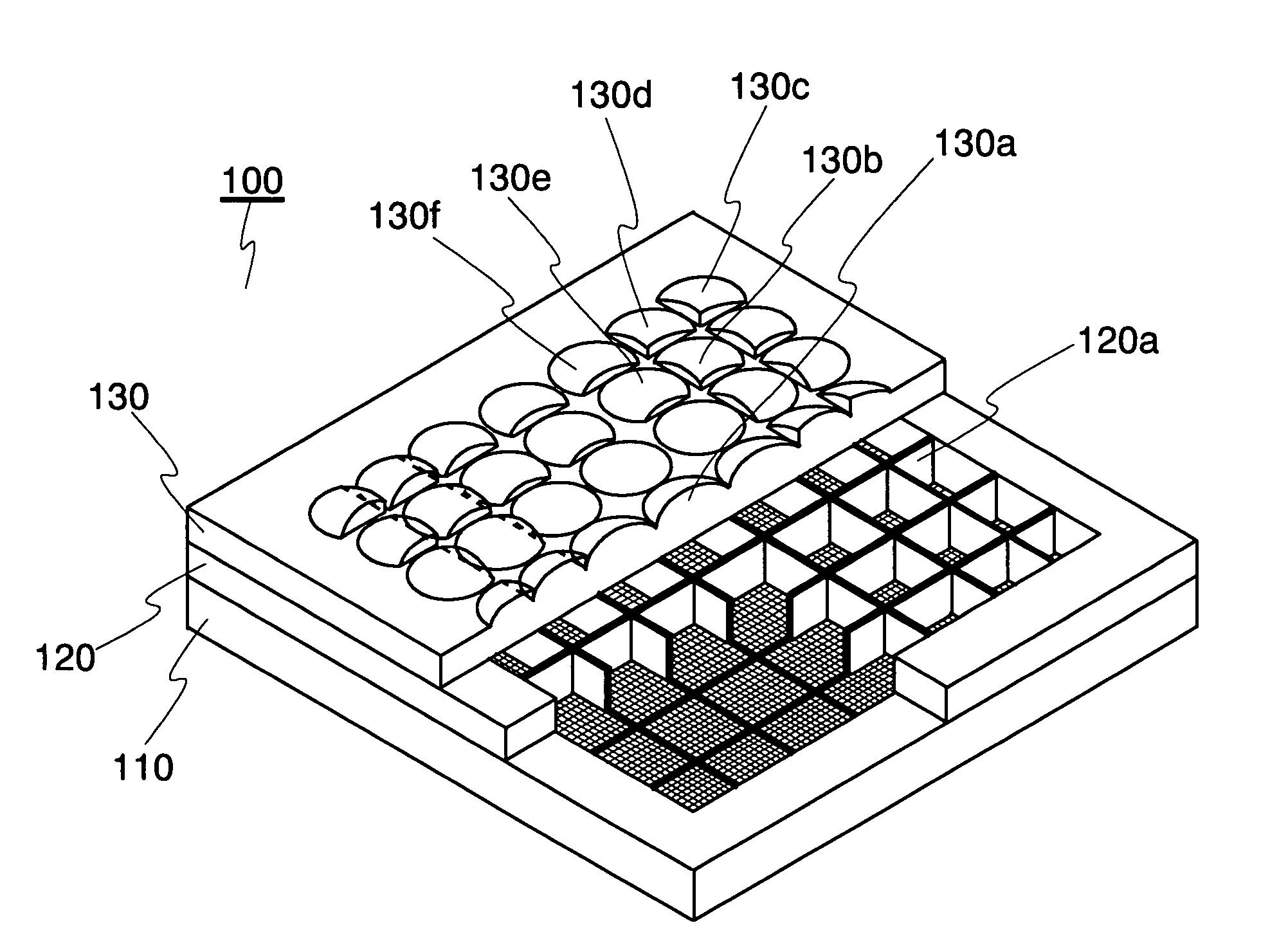
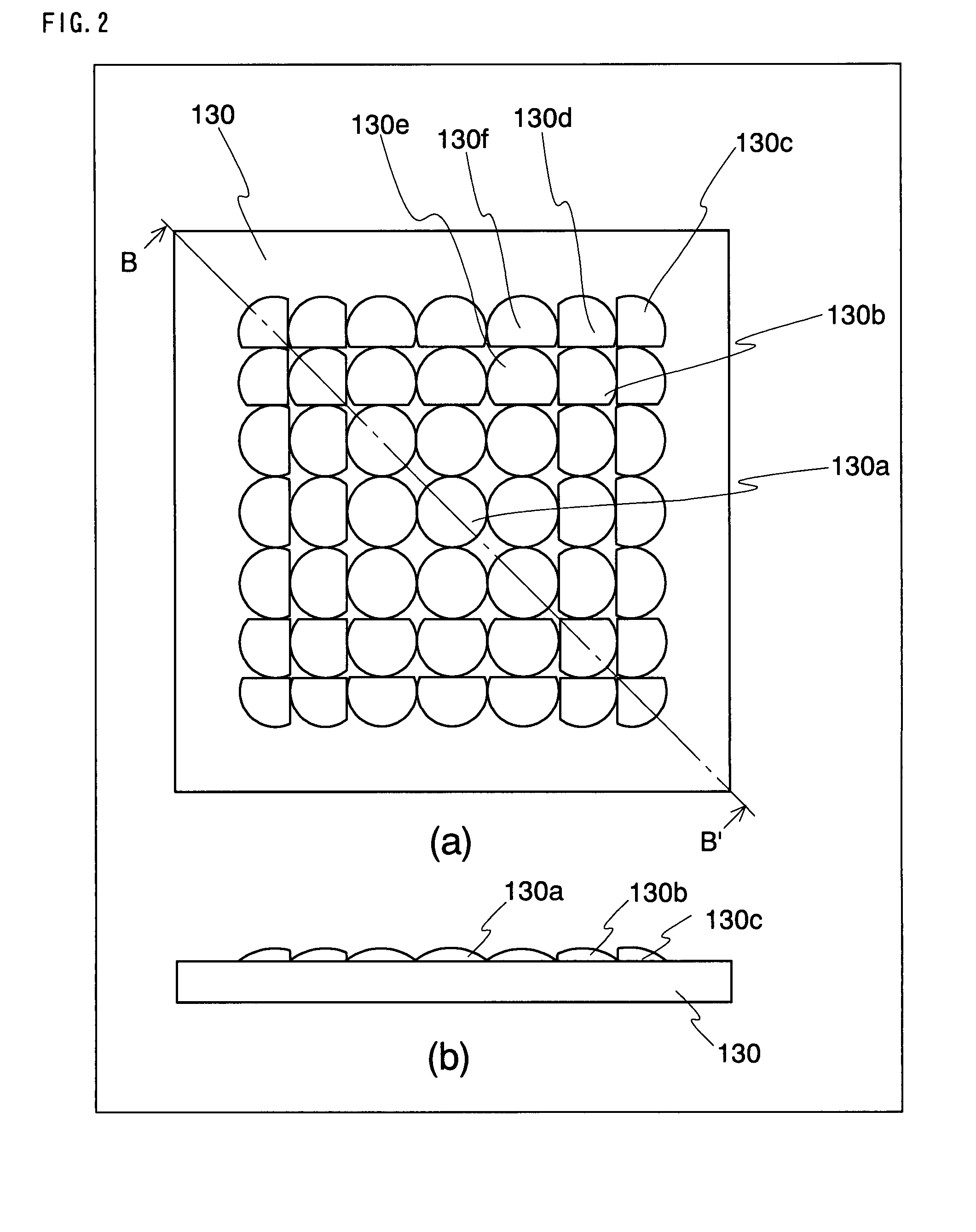
[0043]FIG. 1 is a part-removed perspective view showing a configuration of an imaging device according to Embodiment 1. Further, FIG. 2 is a schematic diagram showing a lens array of the imaging device according to Embodiment 1. FIG. 2(a) is a plan view of the lens array, while FIG. 2(b) is a side view of the lens array. In FIG. 1, the imaging device 100 includes an image sensor 110, a partition member 120 and a lens array 130.

[0044]The image sensor 110 has a light acceptance surface composed of a large number of photoelectric conversion sections each corresponding to a pixel. The image sensor 110 converts incident light that is incident on the light acceptance surface, into an electric signal in accordance with the intensity, and then outputs the signal as an electric image signal to the outside. The light acceptance surface of the image sensor 110 includes rectangular imaging regions 110a to 110f (numerals are not indicated in FIG. 1) and the like each composed of a plurality of p...

embodiment 2

[0062]FIG. 4 is a part-removed perspective view showing a configuration of an imaging device according to Embodiment 2. Further, FIG. 5 is a schematic diagram showing a lens array of an imaging device according to Embodiment 2. FIG. 5(a) is a plan view of the lens array, while FIG. 5(b) is a side view of the lens array. The imaging device 200 according to Embodiment 2 has the same basic configuration as the imaging device 100 according to Embodiment 1. Thus, hereinafter, parts having a new feature depending on a difference point are solely described. In FIG. 4, the imaging device 200 includes an image sensor 210, a partition member 220 and a lens array 230.

[0063]A feature of the imaging device 200 is that all imaging units have a lens element provided with an optical axis in agreement with the axis passing through the center of the corresponding imaging region and have an axial symmetric lens face having the shape of a circle approximately inscribing the imaging region. That is, in ...

embodiment 3

[0071]FIG. 7 is a part-removed perspective view showing a configuration of an imaging device according to Embodiment 3. Further, FIG. 8 is a schematic diagram showing a lens array of an imaging device according to Embodiment 3. FIG. 8(a) is a plan view of the lens array, while FIG. 8(b) is a side view of the lens array. The imaging device 300 according to Embodiment 3 has the same basic configuration as the imaging device 100 according to Embodiment 1. Thus, hereinafter, parts having a new feature depending on a difference part are solely described.

[0072]In the imaging device 300, the image sensor 110 and the partition member 120 have the same structures as those of the imaging device 100. Thus, the imaging device 300 is constructed such that the areas of the imaging regions of imaging units located in the periphery part distant from the center part of the image sensor should be smaller than the areas of the imaging regions of imaging units located in the center part of the image se...


PUM


Abstract

An object of the present invention is to provide: a thin imaging device in which a high image resolution is obtained and in which the resolution does not uniformly vary even when the shooting distance is changed; and a lens array used therein. The present invention relates to an imaging device comprising: a lens array 130 constructed by arranging in parallel a plurality of lens elements having optical power in at least one surface; and an image sensor 110 in which an optical image formed by an optical system having each of the lens elements is received by each of mutually different imaging regions each having a plurality of photoelectric conversion sections so that the optical image is converted into an electric image signal, wherein each lens element and the imaging region corresponding to the lens element constitute an imaging unit, while the imaging units have diverse imaging region areas. The present invention relates also to a lens array used therein.

Description

RELATED APPLICATIONS[0001]This application is the U.S. National Phase under 35 U.S.C. §371 of International Application No. PCT / JP2006 / 305511, filed on Mar. 20, 2006, which in turn claims the benefit of Japanese Application No. 2005-086347, filed on Mar. 24, 2005, the disclosures of which Applications are incorporated by reference herein.TECHNICAL FIELD[0002]The present invention relates to an imaging device. More specifically, the present invention relates to a compound eye type imaging device that includes: a lens array composed of a plurality of lens elements; and an image sensor having imaging regions divided for each lens element. Further, the present invention relates to a lens array used suitably in the imaging device.BACKGROUND ART[0003]In the digital still camera market which is growing in recent years, needs for small thin cameras having improved portability are increasing. In the circuit elements that perform signal processing, function improvement and size reduction are ...

Claims


Application Information

Patent Timeline
Patent Type & Authority Patents(United States)
IPC IPC(8): G02B13/16G02B3/00H01L27/14H04N5/225H04N5/335H04N5/369H04N101/00
CPCG02B3/0043G02B3/005G02B27/1066G02B27/123H01L27/14627H04N5/2254G02B3/0031G02B3/0056G02B3/0075
Inventor YAMAGATA, MICHIHIROOKAYAMA, HIROAKIBOKU, KAZUTAKETANAKA, YASUHIROHAYASHI, KENICHIFUSHIMI, YOSHIMASAMURATA, SHIGEKIHAYASHI, TAKAYUKI
Owner PANASONIC CORP
Why Eureka
Try Eureka