Single-photon avalanche diode and three-dimensional CMOS (Complementary Metal Oxide Semiconductor) image sensor based on same

A single-photon avalanche and diode technology, applied in the field of electronic technology and photoelectric imaging, can solve the problems of premature breakdown of the PN junction, uniformity of photosensitive gain, difficulty in improving image resolution, and failure to improve image quality, etc., to achieve weakening of the edge Effects of premature breakdown, improved light absorption efficiency, and improved gain uniformity

Inactive Publication Date: 2010-12-29
XIANGTAN UNIV
View PDF4 Cites 32 Cited by
  • Summary
  • Abstract
  • Description
  • Claims
  • Application Information

AI Technical Summary

Problems solved by technology

However, if the area of ​​the single photon avalanche diode is continuously reduced to increase the resolution, the signal-to-noise ratio (SNR) will decrease and the crosstalk rate will increase. This will not only fail to improve the image quality, but will cause a decrease in image quality
[0007] To sum up, although the 3D image sensor using single photon avalanche diode as the photosensitive device has great advantages compared with the traditional 3D imaging technology, it still has the photosensitive problem caused by the premature breakdown of the edge of the PN junction. Defects such as poor gain uniformity and difficulty in improving image resolution

Method used


Image

  • Single-photon avalanche diode and three-dimensional CMOS (Complementary Metal Oxide Semiconductor) image sensor based on same
  • Single-photon avalanche diode and three-dimensional CMOS (Complementary Metal Oxide Semiconductor) image sensor based on same
  • Single-photon avalanche diode and three-dimensional CMOS (Complementary Metal Oxide Semiconductor) image sensor based on same

Examples


Embodiment Construction

[0033] The present invention will be further described in detail below in conjunction with the accompanying drawings and embodiments.

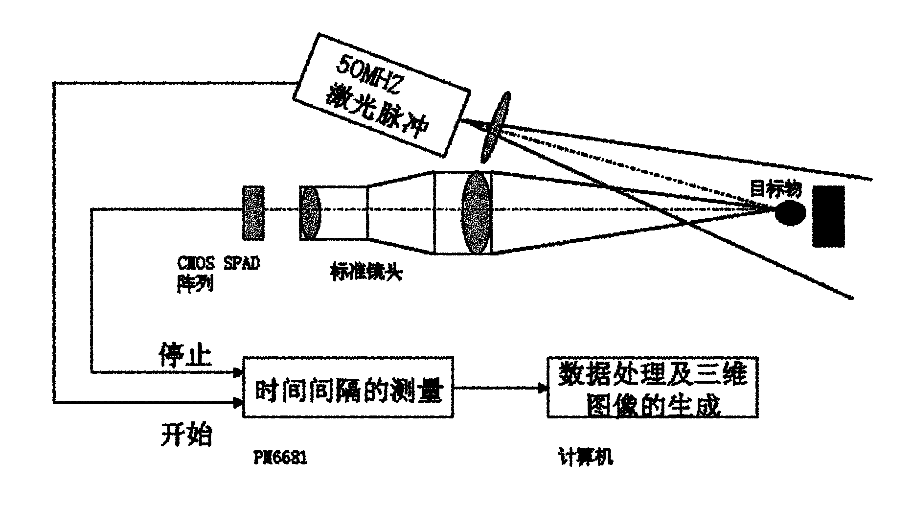
[0034] see figure 1 , is a schematic flowchart of the principle of an imaging system with a three-dimensional CMOS image sensor. Apply the three-dimensional CMOS image sensor of the present invention to figure 1 The imaging system shown provides a convenient and simple method of pixel interpolation. from figure 1 As can be seen in the figure, the imaging system has a three-dimensional CMOS image sensor, which is used to capture images and generate image data including pixel values; a laser emission source, which is used to provide a cone-shaped laser beam with high consistency and suitable wavelength The light beam is irradiated on the target object; the time digital decoder is used to measure the time interval between laser emission and detection by the three-dimensional CMOS image sensor; the image processing unit is used for receiving im...


PUM


Abstract

The invention belongs to the technical field of electronic technologies and photoelectronic imaging technologies, in particular relates to a single-photon avalanche diode and a three-dimensional CMOS (Complementary Metal Oxide Semiconductor) image sensor based on the diode. The single-photon avalanche diode of the invention improves the traditional rectangular photosensitive PN junction into a regular octagon and can conveniently and simply weaken edge breakdown and improve gain uniformity. A two-dimensional pixel array of the three-dimensional CMOS image sensor based on the diode comprises unit pixels of the regular octagon-shaped single-photon avalanche diode and is arrayed in a honeycomb-shape, thereby being convenient for interpolation and improving resolution in horizontal and vertical direction.

Description

technical field [0001] The invention belongs to the field of electronic technology and photoelectric imaging technology, and in particular relates to a single photon avalanche diode and a three-dimensional CMOS image sensor based on the diode. Background technique [0002] As an important photodetection device, avalanche photodiode has a wide range of applications. It can be applied in communication, ranging, three-dimensional imaging and other fields. When the avalanche photodiode is in the working mode, it is required that the reverse voltage applied to both ends of the avalanche photodiode be higher than the avalanche breakdown voltage to obtain a higher avalanche gain. In the planar manufacturing process of the PN junction of the avalanche photodiode, the impurity atoms diffuse to the substrate through the window of the mask. In the traditional avalanche photodiode, a rectangular mask is used, so there are four sharp corners of 90 degrees. In these sharp places of the ...

Claims


Application Information

Patent Timeline
Patent Type & Authority Applications(China)
IPC IPC(8): H01L31/107H01L31/0352H01L31/18H01L27/146H04N5/335
CPCY02P70/50
Inventor 金湘亮周晓亚
Owner XIANGTAN UNIV
Why Eureka
Try Eureka