Semiconductor processing system and vaporizer

a technology of semiconductor devices and processing systems, applied in the field of semiconductor devices and vaporizers, can solve the problems of reducing the film thickness of semiconductor devices, deteriorating the yield of wafers or diced chips, and large number of particles on the surface, so as to reduce the number of particles generated

Active Publication Date: 2011-02-08
TOKYO ELECTRON LTD
View PDF11 Cites 15 Cited by
  • Summary
  • Abstract
  • Description
  • Claims
  • Application Information

AI Technical Summary

Benefits of technology

[0008]An object of the present invention is to provide a semiconductor processing system that can decrease the number of particles generated on a substrate treated by a heat process where water vapor is supplied onto the substrate to perform the heat process. Another object of the present invention is to provide a vaporizer usable in the system.

Problems solved by technology

However, where such a unit is used for performing a heat process, a large number of particles are observed on the surface of a wafer treated by the heat process.
These particles deteriorate the yield of the wafer or diced chips, which becomes prominent with a decrease in the film thickness of semiconductor devices and a decrease in the size of patterns.
However, in order to increase the generation amount of water vapor, the catalysis needs to be increased and thereby brings about a high cost, because the catalysis consists mainly of platinum.
Further, according to this water vapor reaction mechanism, if the amount of catalysis is simply increased, the reaction temperature becomes hard to control.
For this reason, it is necessary to increase the volume of a generating portion or the number of generating portions in accordance with the generation amount of water vapor, which is disadvantageous in cost.

Method used


Image

  • Semiconductor processing system and vaporizer
  • Semiconductor processing system and vaporizer
  • Semiconductor processing system and vaporizer

Examples


first embodiment

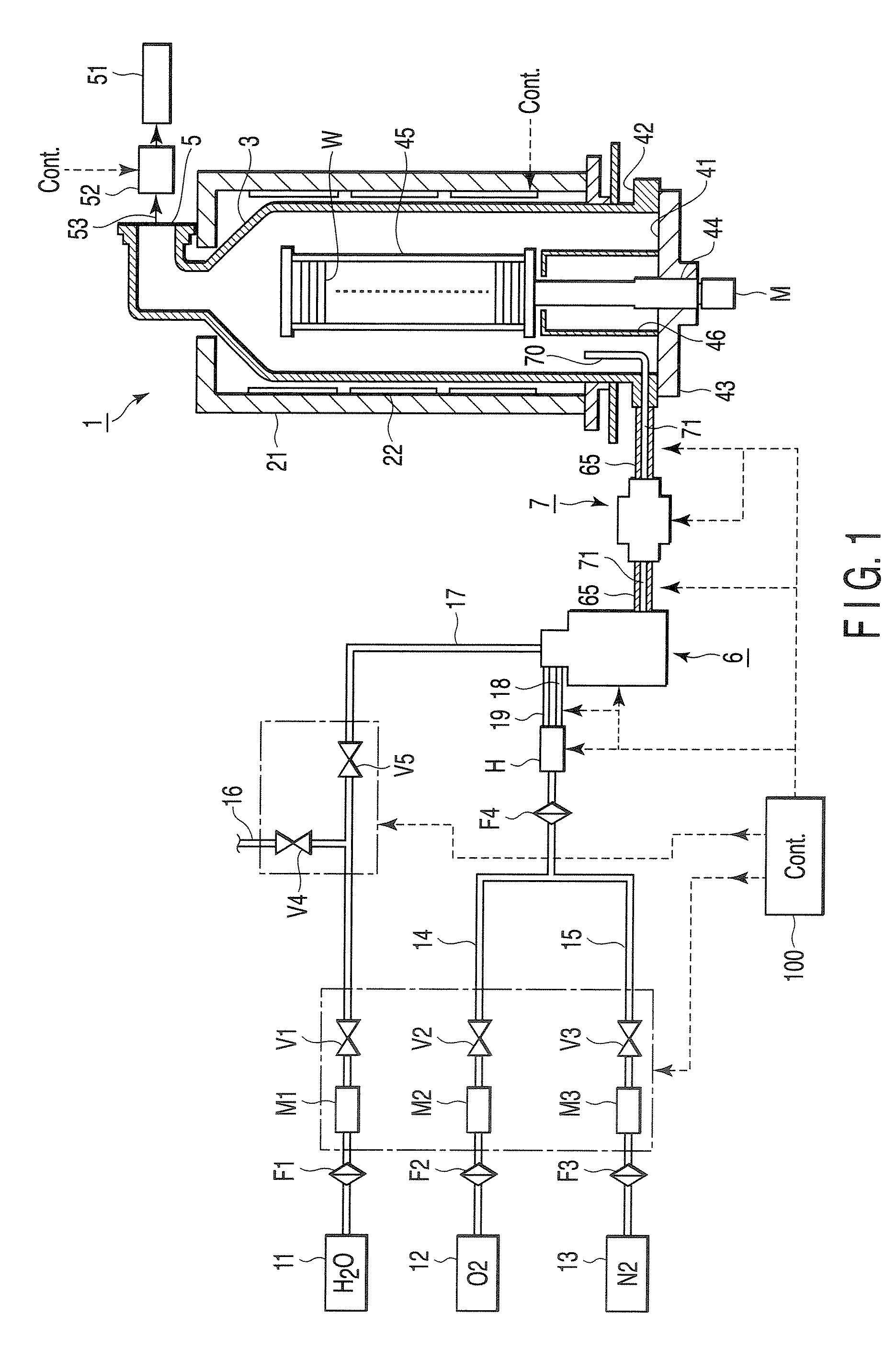
[0037]FIG. 1 is a structural view showing a semiconductor processing system (heat processing apparatus) according to a first embodiment of the present invention. This heat processing system includes a cylindrical reaction container (process chamber) 3, which is made of, e.g., quartz and directed vertically, and a furnace 1 surrounding the reaction container 3. The furnace 1 includes a cylindrical heat-insulating body 21, and a heater 22 disposed on the inner wall of the heat-insulating body 21 and extending in an annular direction. The heater 22 is formed of a plurality of portions controllable independently of each other, which respectively correspond to a plurality of process zones of the process field arrayed in the vertical direction inside the reaction container 3. The portions of the heater 22 are operated for temperature control with reference to temperature measured by temperature detectors, such as thermocouples (not shown), respectively disposed at the process zones.

[0038]...

second embodiment

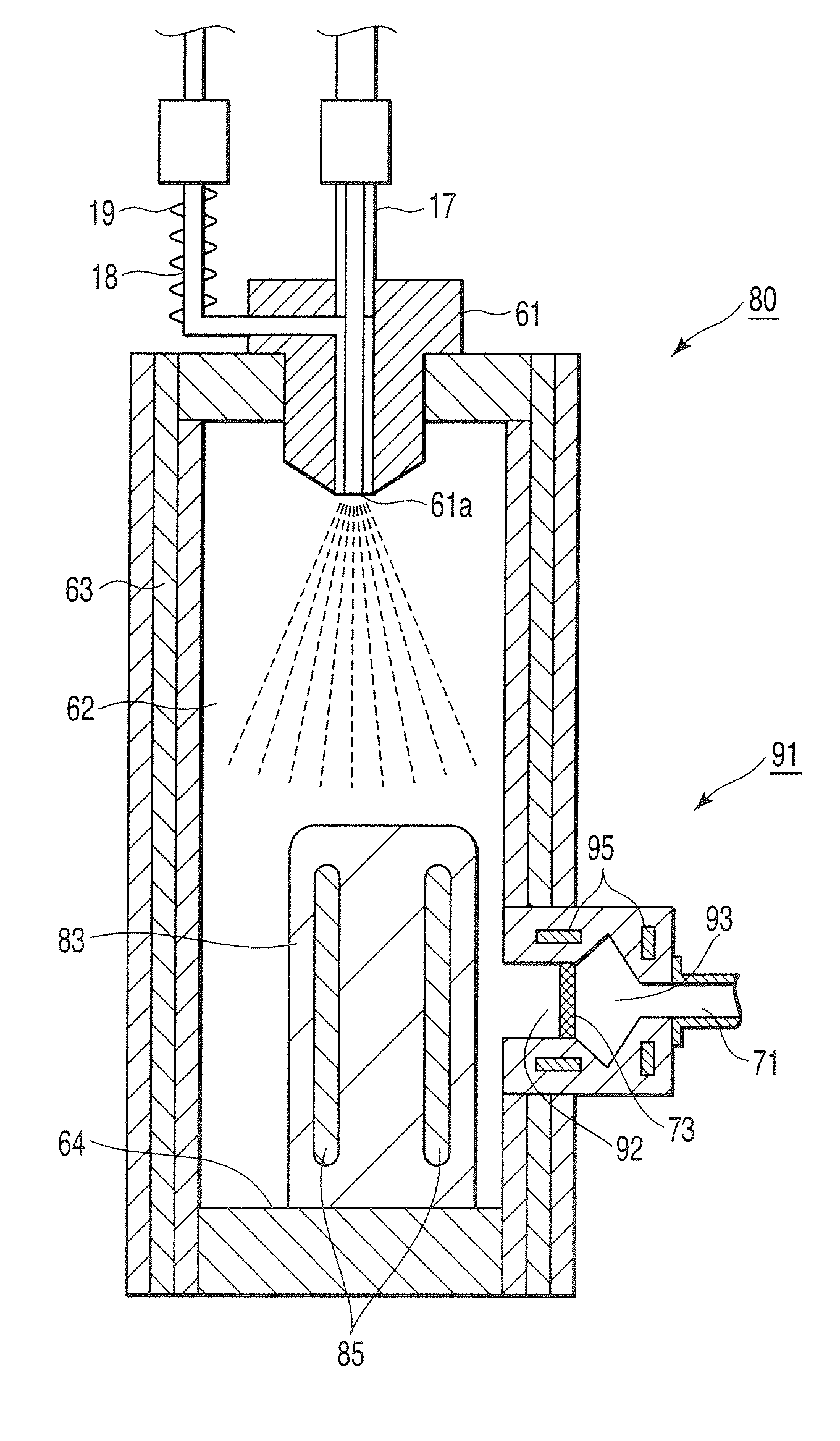
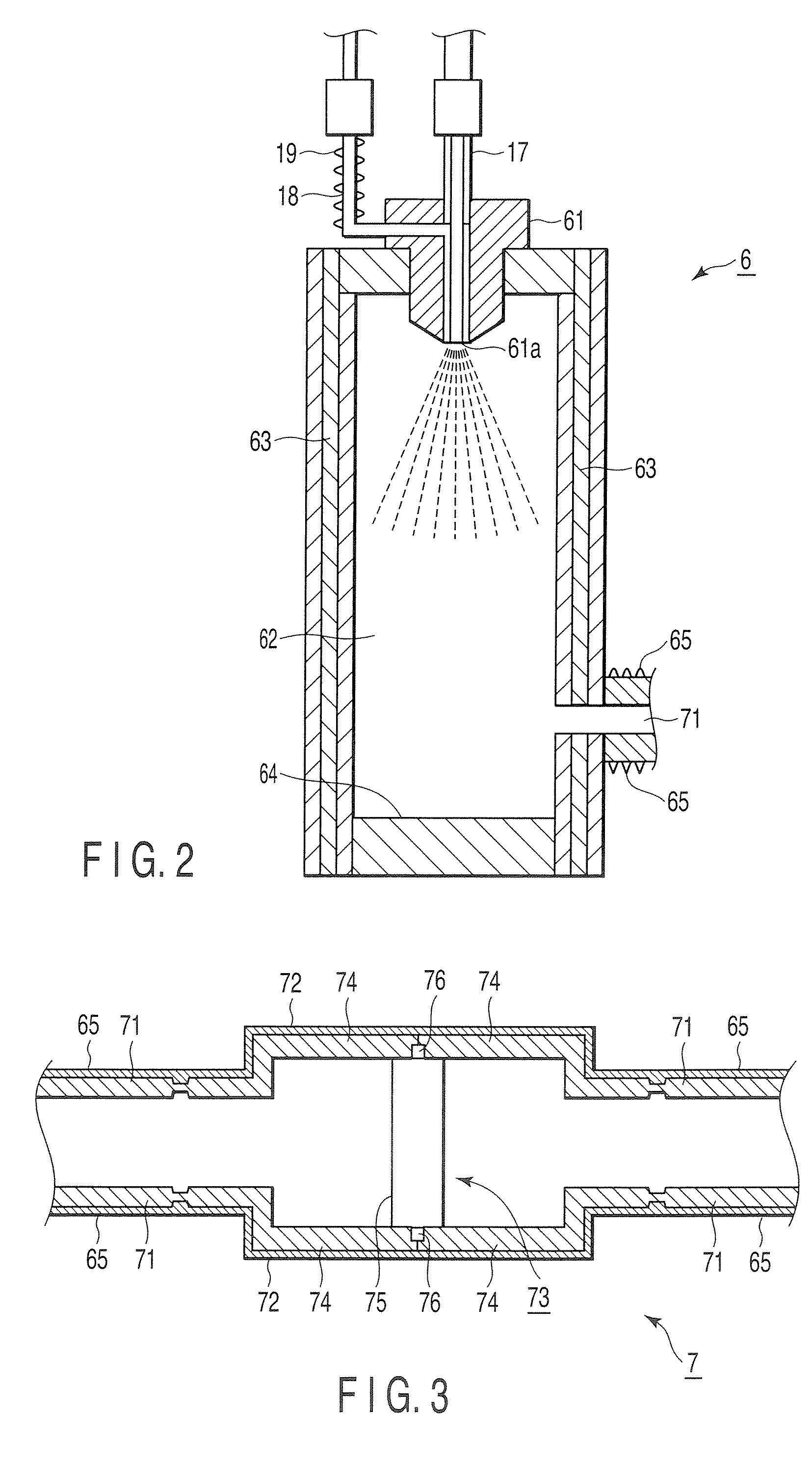
[0072]FIG. 8 is a sectional side view showing a vaporizer used in a semiconductor processing system (heat processing system) according to a second embodiment of the present invention. The vaporizer according to the second embodiment has a structure formed by integrating the first vaporizing section 6 and second vaporizing section 7 of the first embodiment.

[0073]Specifically, this vaporizer includes a container 62 defining a process space of the vaporizer and a port member 91 connected to the sidewall of the container 62 and serving as a water vapor passage. The passage defined by the port member 91 includes first and second portions 92 and 93. The first portion 92 extends outward from the sidewall of the container 62 while keeping an essentially uniform inner diameter. The second portion 93 extends from the distal end of the first portion 92 such that the inner diameter thereof first sharply expands and then sharply contracts. A trapping and vaporizing member 73 structured as descri...


PUM

PropertyMeasurementUnit
diameteraaaaaaaaaa
thicknessaaaaaaaaaa
temperatureaaaaaaaaaa

Abstract

A semiconductor processing system includes a gas supply system configured to supply water vapor into a process chamber that accommodates a target substrate. The gas supply system is provided with a gas generating apparatus for generating water vapor from purified water. The gas generating apparatus includes a first vaporizing section configured to spray the purified water along with a carrier gas and heat the purified water, so as to generate preparatory water vapor containing mist, and a second vaporizing section configured to vaporize mist contained in the preparatory water vapor, so as to generate process water vapor from the preparatory water vapor. In the second vaporizing section, a thin film having a mesh structure is disposed across a passage for the preparatory water vapor and configured to trap mist between the first vaporizing section and the process chamber.

Description

CROSS-REFERENCE TO RELATED APPLICATIONS[0001]This application is based upon and claims the benefit of priority from prior Japanese Patent Applications No. 2005-330357, filed Nov. 15, 2005; and No. 2006-269198, filed Sep. 29, 2006, the entire contents of both of which are incorporated herein by reference.BACKGROUND OF THE INVENTION[0002]1. Field of the Invention[0003]The present invention relates to a semiconductor processing system and a vaporizer for generating water vapor from purified water. The term “semiconductor process” used herein includes various kinds of processes which are performed to manufacture a semiconductor device or a structure having wiring layers, electrodes, and the like to be connected to a semiconductor device, on a target substrate, such as a semiconductor wafer or a glass substrate used for an FPD (Flat Panel Display), e.g., an LCD (Liquid Crystal Display), by forming semiconductor layers, insulating layers, and conductive layers in predetermined patterns on...

Claims


Application Information

Patent Timeline
Patent Type & Authority Patents(United States)
IPC IPC(8): B01F3/04
CPCF22B1/287F22B1/30H01L21/67109Y10S261/65H01L21/02
Inventor OKABE, TSUNEYUKIOKURA, SHIGEYUKI
Owner TOKYO ELECTRON LTD
Why Eureka
Try Eureka