Check patentability & draft patents in minutes with Patsnap Eureka AI!

Semiconductor device having reduced polysilicon pattern width and method of manufacturing the same

a technology of polysilicon and reducing polysilicon, which is applied in the direction of semiconductor devices, basic electric elements, electrical equipment, etc., can solve the problems of increasing process cost and not yet establishing advanced process conditions, and achieve the effect of reducing process cos

Inactive Publication Date: 2011-02-08
DONGBU HITEK CO LTD
View PDF6 Cites 5 Cited by
  • Summary
  • Abstract
  • Description
  • Claims
  • Application Information

AI Technical Summary

Benefits of technology

This approach effectively reduces gate CD, enhances device performance, and decreases manufacturing costs by utilizing standard photolithography equipment, while maintaining signal integrity through the use of spacers and silicide layers to manage contact resistance.

Problems solved by technology

However, since the photolithography process apparatus having the ArF light source is expensive, the process cost is increased.
However, such advanced process conditions have not yet been established.

Method used


Image

  • Semiconductor device having reduced polysilicon pattern width and method of manufacturing the same
  • Semiconductor device having reduced polysilicon pattern width and method of manufacturing the same
  • Semiconductor device having reduced polysilicon pattern width and method of manufacturing the same

Examples


Embodiment Construction

[0014]Hereinafter, an embodiment of the present invention will be described with reference to the accompanying drawings. When the terms “on” or “over” are used herein, when referring to layers, regions, patterns, or structures, it is understood that the layer, region, pattern or structure can be directly on another layer or structure, or intervening layers, regions, patterns, or structures may also be present. When the terms “under” or “below” are used herein, when referring to layers, regions, patterns, or structures, it is understood that the layer, region, pattern or structure can be directly under the other layer or structure, or intervening layers, regions, patterns, or structures may also be present.

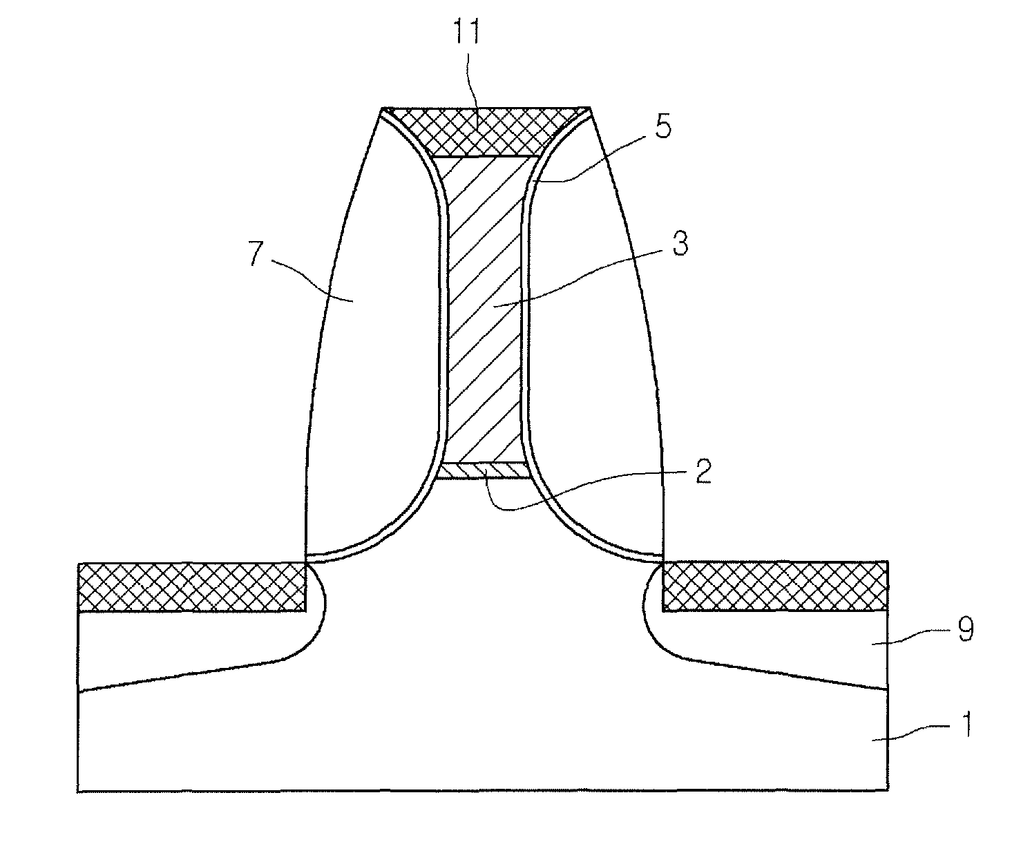
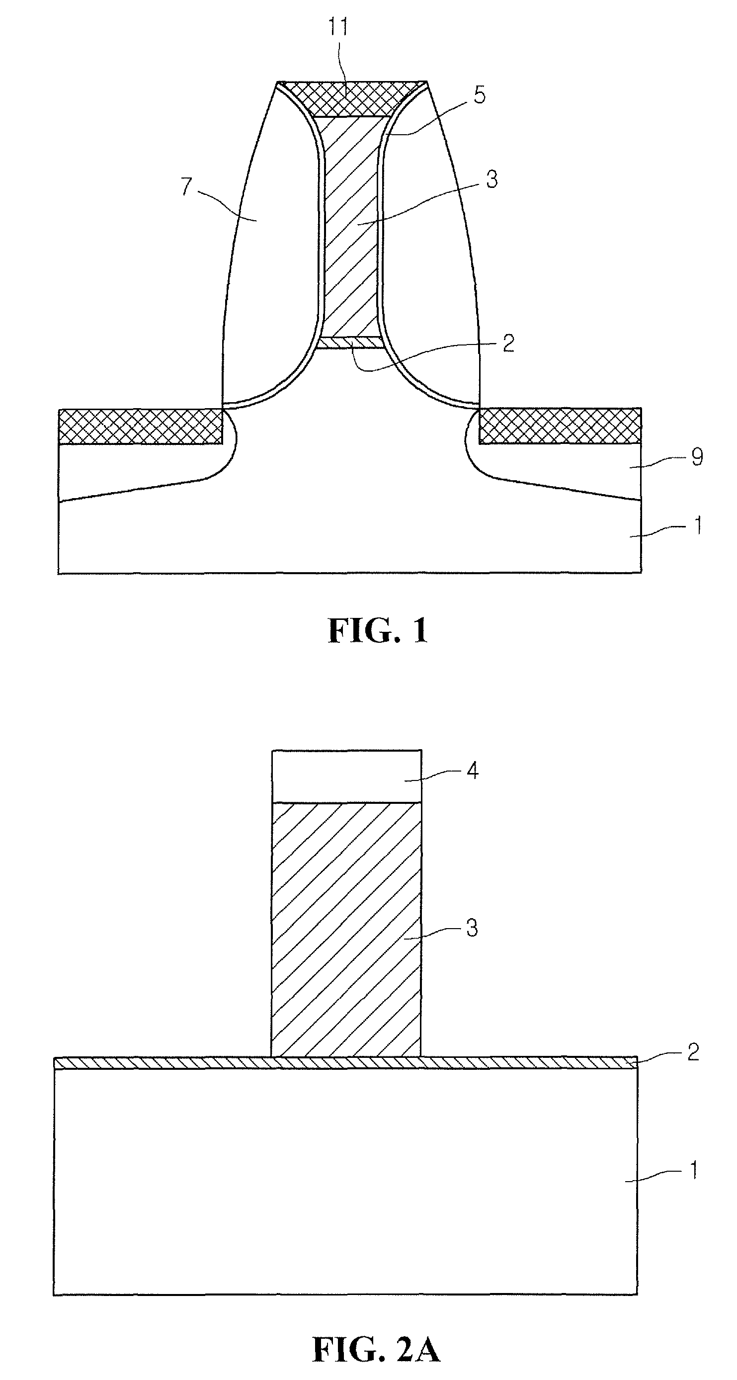
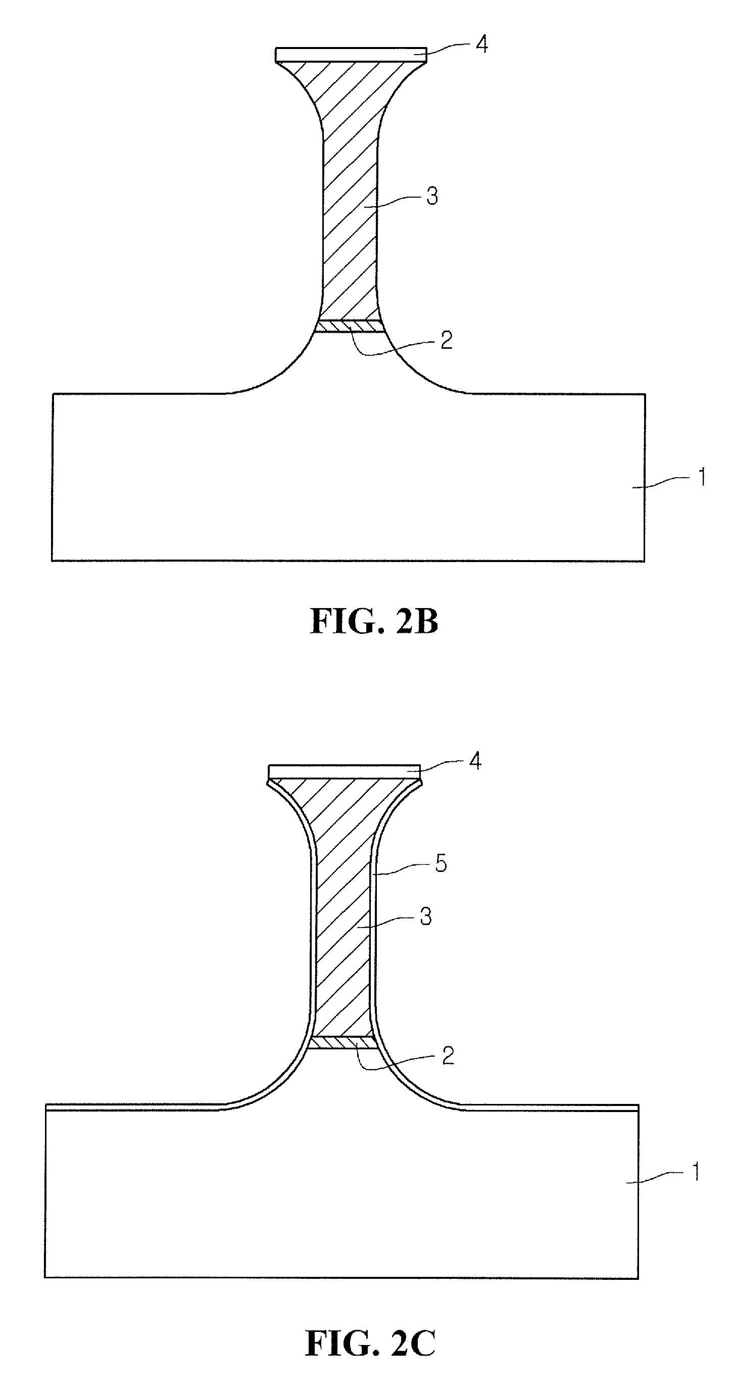
[0015]Referring to FIG. 1, a transistor having a gate with a reduced critical dimension (CD) can be provided. The transistor can include a gate oxide layer 2 and a polysilicon layer 3 on a substrate 1.

[0016]The polysilicon layer 3 can be formed such that the width of the upper port...


PUM


Abstract

Disclosed is a method of manufacturing a semiconductor device. The method comprises consecutively depositing and patterning polysilicon and mask material on a substrate to form a polysilicon layer and a mask layer, reducing a width of the polysilicon layer, depositing and etching insulating material on the substrate to form a spacer on a lateral side of the polysilicon layer, and forming a source / drain region in the substrate at sides of the spacer.

Description

CROSS-REFERENCE TO RELATED APPLICATION[0001]The present application claims the benefit under 35 U.S.C. §119 of Korean Patent Application No. 10-2006-0118810, filed Nov. 29, 2006, which is hereby incorporated by reference in its entirety.BACKGROUND[0002]The performance of a semiconductor device is greatly affected by the Critical Dimension (CD) of a gate. That is, as the CD of the gate is shortened, gate signals are transmitted well, so the desired functions of the device can be performed without errors. Further, as the CD of the gate is shortened, the size of the device is reduced, so the device can be highly integrated.[0003]Accordingly, research has been actively studied to shorten the CD of the gate in the semiconductor device.[0004]The CD of the gate can be determined depending on the efficiency of photolithography and etching processes.[0005]Accordingly, in order to precisely form the CD of the gate, various attempts are introduced in the photolithography and etching processes....

Claims


Application Information

Patent Timeline
Patent Type & Authority Patents(United States)
IPC IPC(8): H01L21/336H01L21/461H01L21/8234H01L21/44
CPCH01L21/28035H01L21/28123H01L21/28247H01L29/42376H01L29/4916H01L29/66575H01L29/66636H01L29/78H01L29/665
Inventor HONG, JI HO
Owner DONGBU HITEK CO LTD
Features
  • R&D
  • Intellectual Property
  • Life Sciences
  • Materials
  • Tech Scout
  • Unparalleled Data Quality
  • Higher Quality Content
  • 60% Fewer Hallucinations
Learn More