Semiconductor apparatus

a technology of nitride semiconductor and semiconductor, applied in the direction of electrical devices, semiconductor devices, diodes, etc., can solve the problems of low resistance and power devices such as avalanche capability not being taken into account, and achieve the effect of higher resistan

Inactive Publication Date: 2011-02-08
KK TOSHIBA
View PDF15 Cites 112 Cited by
  • Summary
  • Abstract
  • Description
  • Claims
  • Application Information

AI Technical Summary

Problems solved by technology

However, while GaN and other nitride semiconductor devices achieve low on-resistance, characteristics specific to power devices such as avalanche capability are not taken into consideration in their design.

Method used


Image

  • Semiconductor apparatus
  • Semiconductor apparatus
  • Semiconductor apparatus

Examples


first embodiment

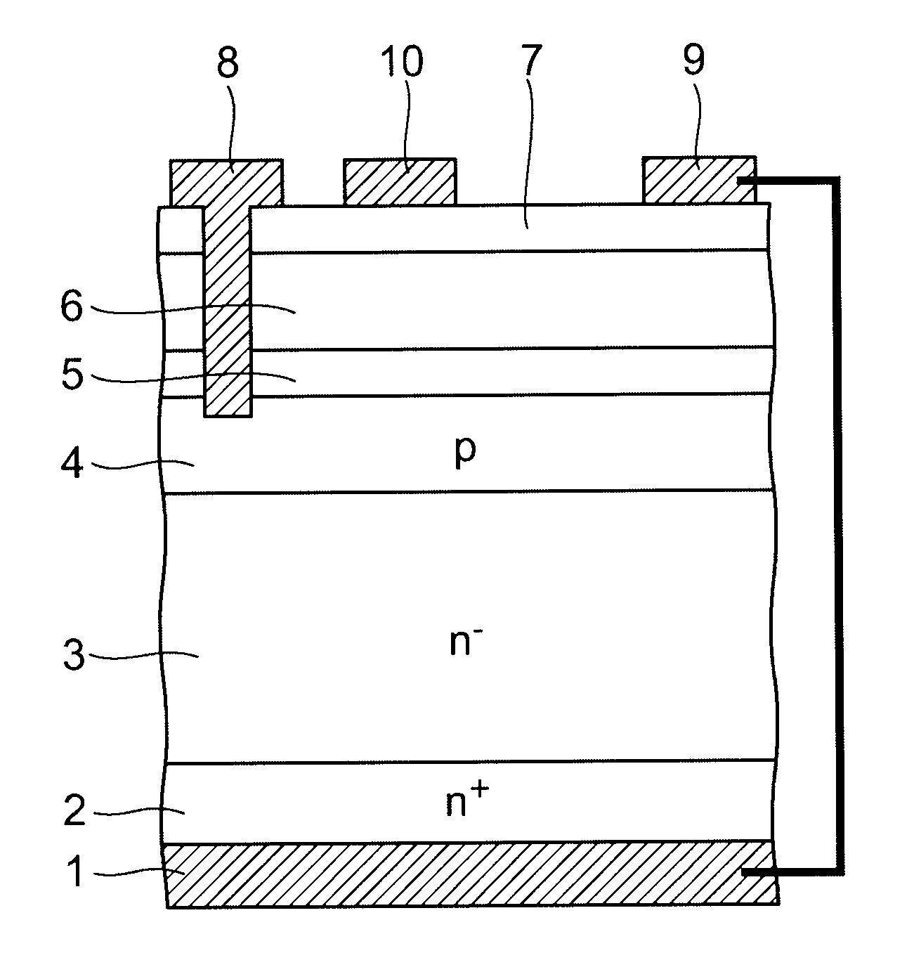
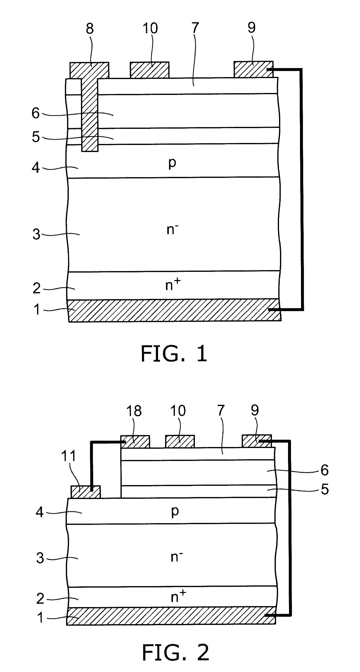
[0020]FIG. 1 is a schematic view showing the principal cross-sectional structure of a semiconductor apparatus according to a first embodiment of the invention.

[0021]On the major surface of a highly doped n+-type silicon layer (or silicon substrate) 2 serving as a first silicon layer, an n−-type silicon layer 3 is provided as a second silicon layer. A p-type silicon layer 4 is provided as a third silicon layer on the major surface of the n−-type silicon layer 3. The n−-type silicon layer 3 has a lower impurity concentration and a higher resistance than the n+-type silicon layer 2 and the p-type silicon layer 4.

[0022]A heterojunction structure of a channel layer 6 serving as a first nitride semiconductor layer and a barrier layer 7 serving as a second nitride semiconductor layer, which has a larger bandgap than the channel layer 6, is provided via a buffer layer 5 on the major surface of the p-type silicon layer 4.

[0023]For example, the channel layer 6 is made of undoped GaN, and the ...

second embodiment

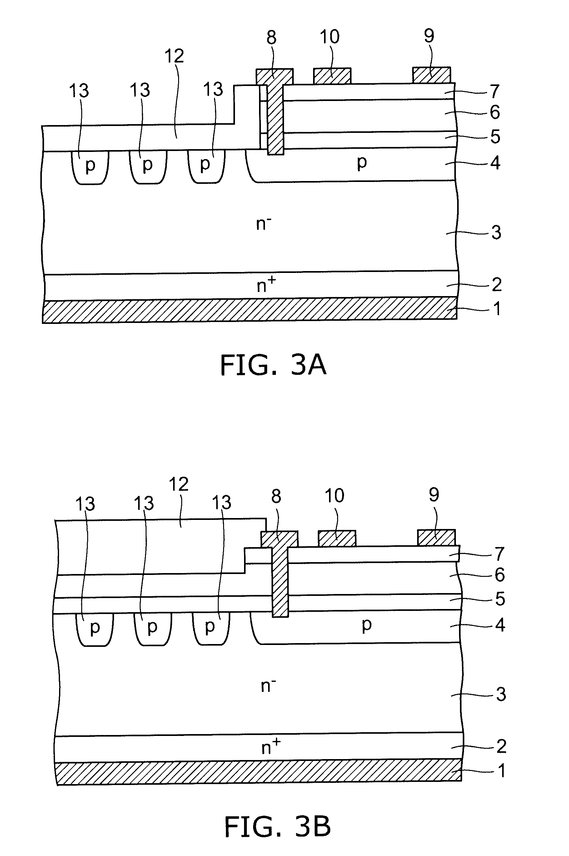
[0035]FIG. 3A is a schematic view showing the principal cross-sectional structure of a semiconductor apparatus according to a second embodiment of the invention.

[0036]In this embodiment, one or more (in the example shown, three) p-type guard ring layers 13 are selectively provided as fourth silicon layers in the surface of the n−-type silicon layer 3 in the termination section, which is located on the outer periphery side of the device section including the pin diode and the overlying HFET. The surface of the termination section including the guard ring layers 13 is covered with a field insulating film 12.

[0037]Thus, even if a depletion layer extends from the p-type silicon layer 4 of the device section toward the termination section, the guard ring layer 13 prevents electric field concentration at the end of the p-type silicon layer 4, achieving stable breakdown voltage. Furthermore, prevention of electric field concentration at the end of the p-type silicon layer 4 allows an avala...

third embodiment

[0042]FIG. 4 is a schematic view showing the principal cross-sectional structure of a semiconductor apparatus according to a third embodiment of the invention.

[0043]In this embodiment, an insulator 14 such as silicon oxide and silicon nitride is provided between the channel layer 6 and the n−-type silicon layer 3 below the drain electrode 9. In this structure, when a high voltage is applied to the drain electrode 9, the voltage is also applied to the insulator 14. Thus, the voltage is held by both the channel layer 6 and the insulator 14. Hence, the channel layer 6 does not need to be so thickened for the purpose of ensuring adequate breakdown voltage. Because the channel layer 6 can be thinned, a crack-free AlGaN / GaN heterojunction structure of the barrier layer 7 and the channel layer 6 can be easily formed, and the substrate warpage can be also reduced.

[0044]The structure shown in FIG. 4 can be realized by forming a groove extending from the surface of the p-type silicon layer 4 ...


PUM


Abstract

A semiconductor apparatus includes, a first silicon layer of a first conductivity type; a second silicon layer provided on the first silicon layer and having a higher resistance than the first silicon layer, a third silicon layer of a second conductivity type provided on the second silicon layer, a first nitride semiconductor layer provided on the third silicon layer, a second nitride semiconductor layer provided on the first nitride semiconductor layer and having a larger bandgap than the first nitride semiconductor layer, a first main electrode being in contact with a surface of the second nitride semiconductor layer and connected to the third silicon layer, a second main electrode being in contact with the surface of the second nitride semiconductor layer and connected to the first silicon layer, and a control electrode provided between the first main electrode and the second main electrode on the second nitride semiconductor layer.

Description

CROSS-REFERENCE TO RELATED APPLICATIONS[0001]This application is based upon and claims the benefit of priority from the prior Japanese Patent Application No. 2007-167427, filed on Jun. 26, 2007; the entire contents of which are incorporated herein by reference.BACKGROUND OF THE INVENTION[0002]1. Field of the Invention[0003]This invention relates to a semiconductor apparatus, and more particularly to a semiconductor apparatus based on a heterojunction structure of a nitride semiconductor.[0004]2. Background Art[0005]A nitride semiconductor device based on GaN has a larger bandgap than Si and a higher critical electric field. Hence, a small device with high breakdown voltage is realized more easily. The GaN-based semiconductor device used as a power semiconductor device has low on-resistance, realizing a low-loss device. Among others, a field effect transistor based on AlGaN / GaN heterojunction structure (see, e.g., JP-A 2007-059589 (Kokai)) has a simple device structure, showing promi...

Claims


Application Information

Patent Timeline
Patent Type & Authority Patents(United States)
IPC IPC(8): H01L29/66
CPCH01L29/404H01L29/0619H01L29/7786H01L29/41766H01L27/0688H01L29/402H01L29/0615H01L27/0629H01L21/8258H01L29/2003H01L29/0649H01L29/861H01L29/872H01L29/1075
Inventor SAITO, WATARU
Owner KK TOSHIBA
Why Eureka
Try Eureka