Double-sided connector with protrusions

a double-sided connector and protruding technology, applied in the direction of connection contact material, semiconductor/solid-state device details, coupling device connection, etc., can solve the problems of inability to meet predetermined load, inability to realize finer pitches, and complex manufacturing processes. , to achieve the effect of efficient arrangemen

Inactive Publication Date: 2011-02-15
FUJIKURA LTD
View PDF24 Cites 22 Cited by
  • Summary
  • Abstract
  • Description
  • Claims
  • Application Information

AI Technical Summary

Benefits of technology

[0028]According to the double-sided connector, since the elastomer composing the first face of the insulating member has elasticity, the point of contact part can move across wide range with respect to the first face of the insulating member.
[0029]Further, since the point of contact part is hemispherical, the point of contact part contacts the other conductive member (which is the contact pad of an LGA package or the solder ball of a BGA package) by one point. This enables ensuring sufficient contact pressure since the load can be concentrated only at this point of contact. Moreover, since the point of contact part is hemispherical, it has sufficient rigidity enough to prevent the possibility of being collapsed even when the load is concentrated thereat.
[0030]Since the point of contact part which is the movable portion of the contact terminal part, is at a distance from the through-hole for interlayer conduction, stress will not be concentrated at the point of contact part and the through-hole, and hence there is a low possibility of collapsing them.
[0031]Therefore, the point of contact part can secure a wide movable range without affecting on the design of the point of contact part. This eliminates any possibility of warping of the package and the printed circuit board, absorbs any variations in the height of the contact terminals, and thereby allowing the finer pitches.
[0036]In this case, there is no possibility of causing too wide separation of the sloping part with respect to the first face. Therefore, the contact terminal part can move reliably within a predetermined range with respect to the insulating member.(7) It may be arranged such that: a plurality of the contact terminal parts is provided on at least the first face; and adjacent contact terminal parts are arranged so as to be electrically independent from each other.
[0038]In this case, the contact terminal part and the through-hole can be arranged efficiently in a fixed area.(9) A sidewall of the protrusion may slope with respect to the plane around the protrusion of the first face.

Problems solved by technology

However, since this type of socket contact for an LGA package basically has a cantilever spring structure, it was difficult to realize finer pitches.
If the wire diameter of the cantilever spring portion is reduced to an appropriate value to lower the load to be applied thereon, problems arises such as: the cantilever spring portion will deform in excess of an elastic deformation range thereof, and then will have a plastic deformation, when the predetermined load is applied; and the required allowable stress decreases and this results in incapable of withstanding the predetermined load.
Therefore, the manufacturing processes are consequently complex, and the manufacturing cost thereof is high.
In such case, the wiping effect cannot be expected although it is required as one of the functions of the socket contact.
However, in the above-mentioned structure, the amount of motion for absorbing the warping and variations in the coplanarity is limited by the height of the dome-shaped portion.
Furthermore, in the above-mentioned structure where the metal film is plated on the elastomer, since the movable range of the point of contact part is limited by the range of deformation of the elastomer along its thickness direction, enlargement of the movable range cannot be expected.

Method used


Image

  • Double-sided connector with protrusions
  • Double-sided connector with protrusions
  • Double-sided connector with protrusions

Examples


first embodiment

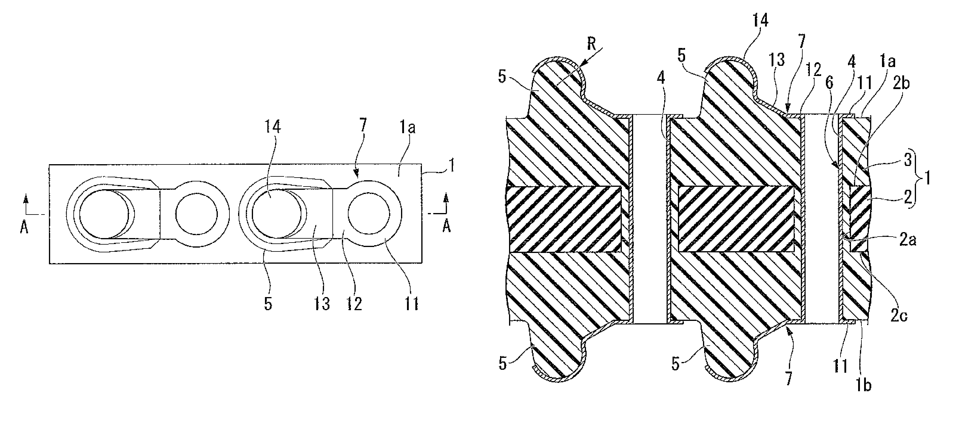
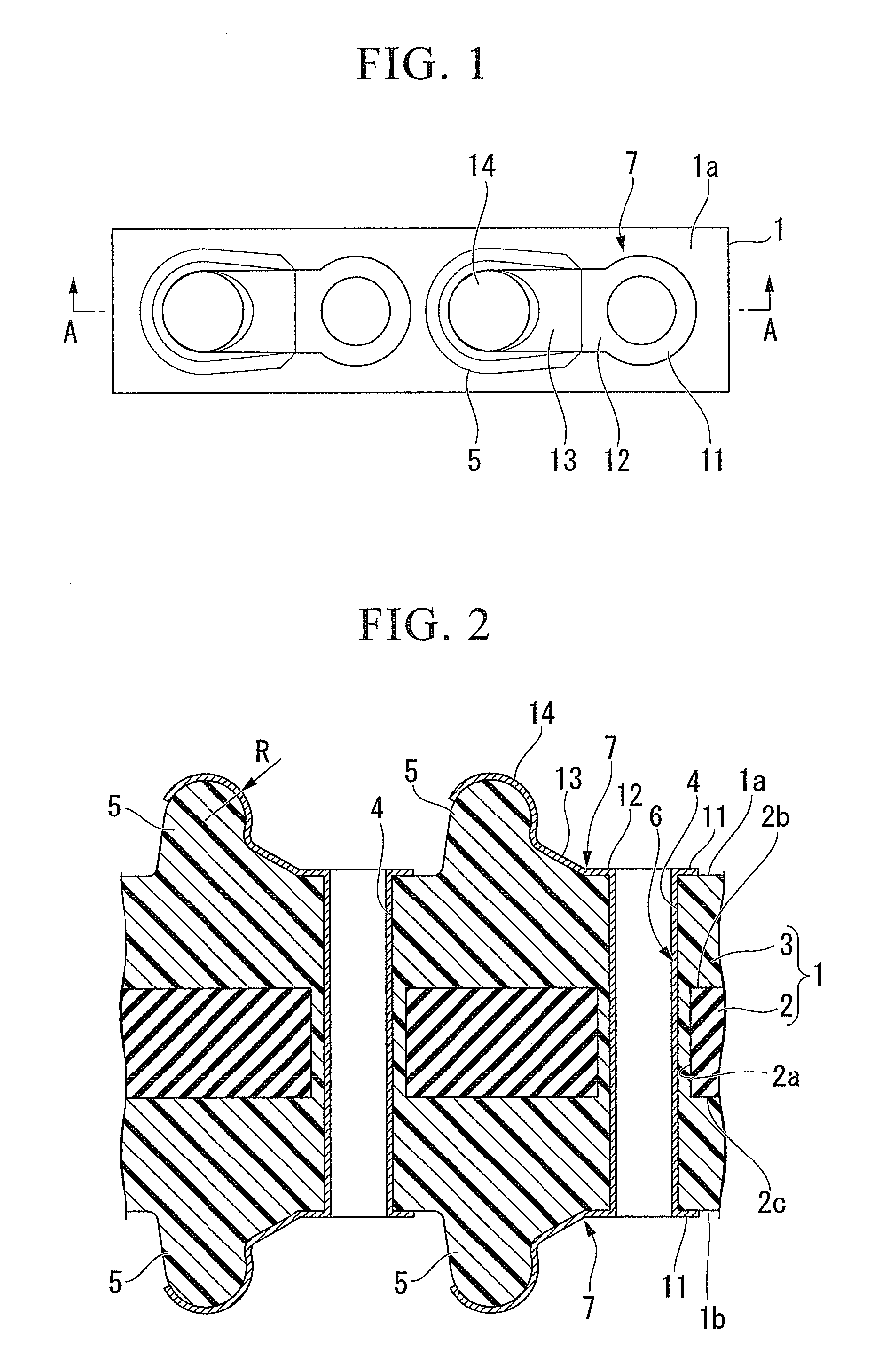
[0049]FIG. 1 is a plan view of a double-sided connector according to a first embodiment of the present invention, and FIG. 2 is a cross-sectional view taken along the line A-A of FIG. 1.

[0050]In these FIGS. 1 and 2, reference numeral 1 represents an insulating member. The insulating member 1 is composed of: an insulating substrate (an insulating material) 2 which has holes 2a which are formed in advance at the positions where through holes 4 are to be formed; and a film or sheet elastomer 3 which is insert-molded with the insulating substrate 2 so as to cover all of a top face 2b, a bottom face 2c, and the holes 2a of the insulating substrate 2, and which has a predetermined thickness.

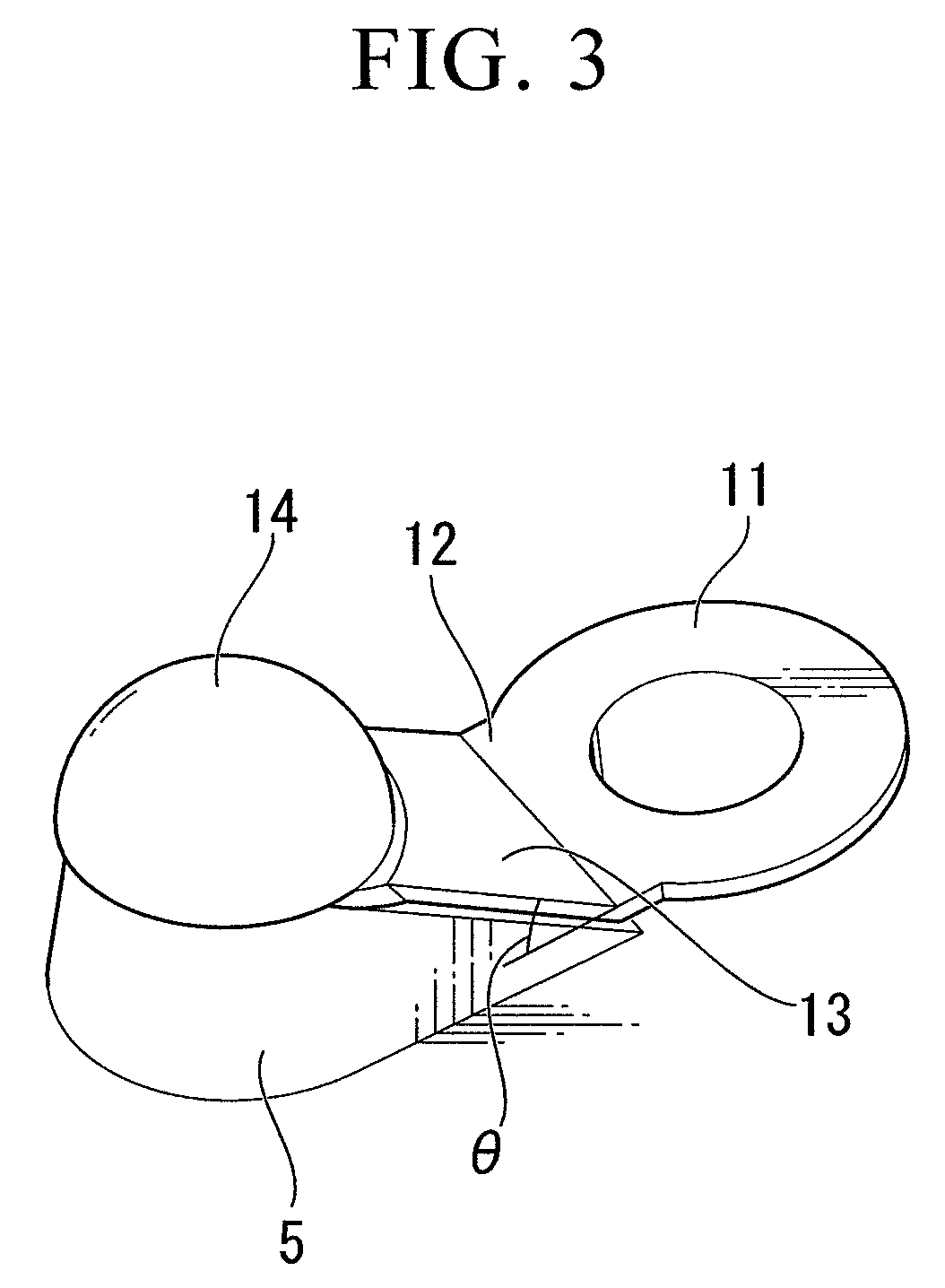
[0051]A plurality of the through-holes 4 (two of them are shown in FIGS. 1 and 2) is formed in the insulating member 1, and penetrates the insulating member in its thickness direction. On a top face 1a and a bottom face 1b of the insulating member 1, approximately hemispherical protrusions 5 made of el...

second embodiment

[0086]FIG. 6 is a plan view of a double-sided connector according to a second embodiment of the present invention.

[0087]The double-sided connector of the present embodiment differs from that of the first embodiment in that the through-holes 4 are arranged in a matrix of four rows and four columns on one face of the insulating member 1 at an inter-terminal pitch P. In addition, each of the contact terminal parts 7 is formed at the corresponding conductive part 6 covering the through-hole 4 and, instead of connecting adjacent contact terminal parts 7, they are formed so as to be independent from each other. When the above-mentioned one face of the insulating member 1 is seen in front view, the angle ø between the extending direction of the contact terminal parts 7 and a side 1c of the insulating member 1 is 45 degrees.

[0088]The inter-terminal pitch P is, for example, 1 mm. In this case, approximately 0.5 mm can be used for the width of the contact terminal part 7, and thus 0.25 mm can...

third embodiment

[0092]FIG. 7 is a plan view of a double-sided connector according to a third embodiment of the present invention. FIG. 8 is a cross-sectional view taken along the line B-B of FIG. 7.

[0093]The double-sided connector of the present embodiment differs from that of the first embodiment in that: a terminal part 31 which is electrically connected to the conductive part 6 is formed near the opening end part of the each through-hole 4 on the bottom face 1b of the insulating member 1; and a soldered part 32 is formed on the each of terminal part 31.

[0094]As shown in this construction where the soldered parts 32 are formed on the bottom face 1b of the insulating member 1, the double-sided connector of the present embodiment can be applied not only for the construction where both of the top face 1a or the bottom face 1b have the point of contact structures, but also for the construction where one of the top face 1a or the bottom face 1b has solder-mounting structure.


PUM


Abstract

A double-sided connector is provided including: an insulating member having an insulating substrate and an elastomer insert-molded on both faces of the insulating substrate, and a through-hole formed along a thickness direction of the insulating substrate and the elastomer; a conductive member formed on an inner face of the through-hole, both ends of the conductive member exposed at the both faces; and a contact terminal part provided at one end of the conductive member. A protrusion is formed on at least a first face of the two faces of the insulating member and near one of the two ends of the through-hole. The protrusion formed by a part of the elastomer protruding from the first face enables an approximately hemispherical point of contact part connected to the sloping part and covering the top.

Description

CROSS-REFERENCE TO RELATED APPLICATIONS[0001]This application claims priority from Japanese Patent Application No. 2008-171004, filed Jun. 30, 2008, the contents of which are incorporated herein by reference.BACKGROUND OF THE INVENTION[0002]1. Field of the Invention[0003]The present invention relates to a double-sided connector that, when an IC package such as a CPU or an LSI, an LGA package, a BGA package or the like is mounted on a printed circuit board, can absorb variations in the height of contact terminals, without generating warping in the package and the printed circuit board.[0004]Priority is claimed on Japanese Patent Application No. 2008-171004, filed Jun. 30, 2008, the contents of which are incorporated herein by reference.[0005]2. Description of Related Art[0006]Conventionally, technology for mounting an integrated circuit (IC) package such as a central processing unit (CPU) or large scale integrated circuit (LSI) on a printed circuit board via a socket has been conside...

Claims


Application Information

Patent Timeline
Patent Type & Authority Patents(United States)
IPC IPC(8): H01R12/00H05K1/00
CPCH01L23/49827H01L24/16H05K3/326H01L24/90H01L2224/13099H01L2224/16H01L2924/01002H01L2924/01013H01L2924/01029H01L2924/01033H01L2924/01046H01L2924/01078H01L2924/01082H01L2924/14H01L2924/30107H05K1/114H05K2201/0133H05K2201/0367H05K2201/10378H01R12/714H01L2924/01005H01L2924/01006H01L2924/01047H01L2224/0554H01L2224/05568H01L2224/05573H01L2924/00014H01L2224/05599H01L2224/0555H01L2224/0556H01R12/57
Inventor NIKAIDO, SHINICHIYAMAGAMI, KATSUYAOUCHI, YASUHIRO
Owner FUJIKURA LTD
Why Eureka
Try Eureka