[0010]Applicants have found that suitable combinations of donors and acceptors may be used to produce enhanced-efficiency, dense film LEEs (where the film dimensionality is 2- or 3-dimensional). The components of the LEE's may be either photo-excited (i.e., an optical barcode, scintillator, optical tag, or an LED color-conversion element wherein the emission of a high-efficiency solid-state LED such as GaN is converted to a desired spectral profile such as white-light), or electrically excited (i.e, a traditional LED where carriers are electrically injected). Rather than seeking to minimize “bad” energy transfer, the present invention utilizes suitable pairs of donors and acceptors, in which donors transfer energy to a given acceptor rather than to any random acceptor that is in proximity. This allows control of energy transfer between donors and acceptors, and results in a number of advantages.
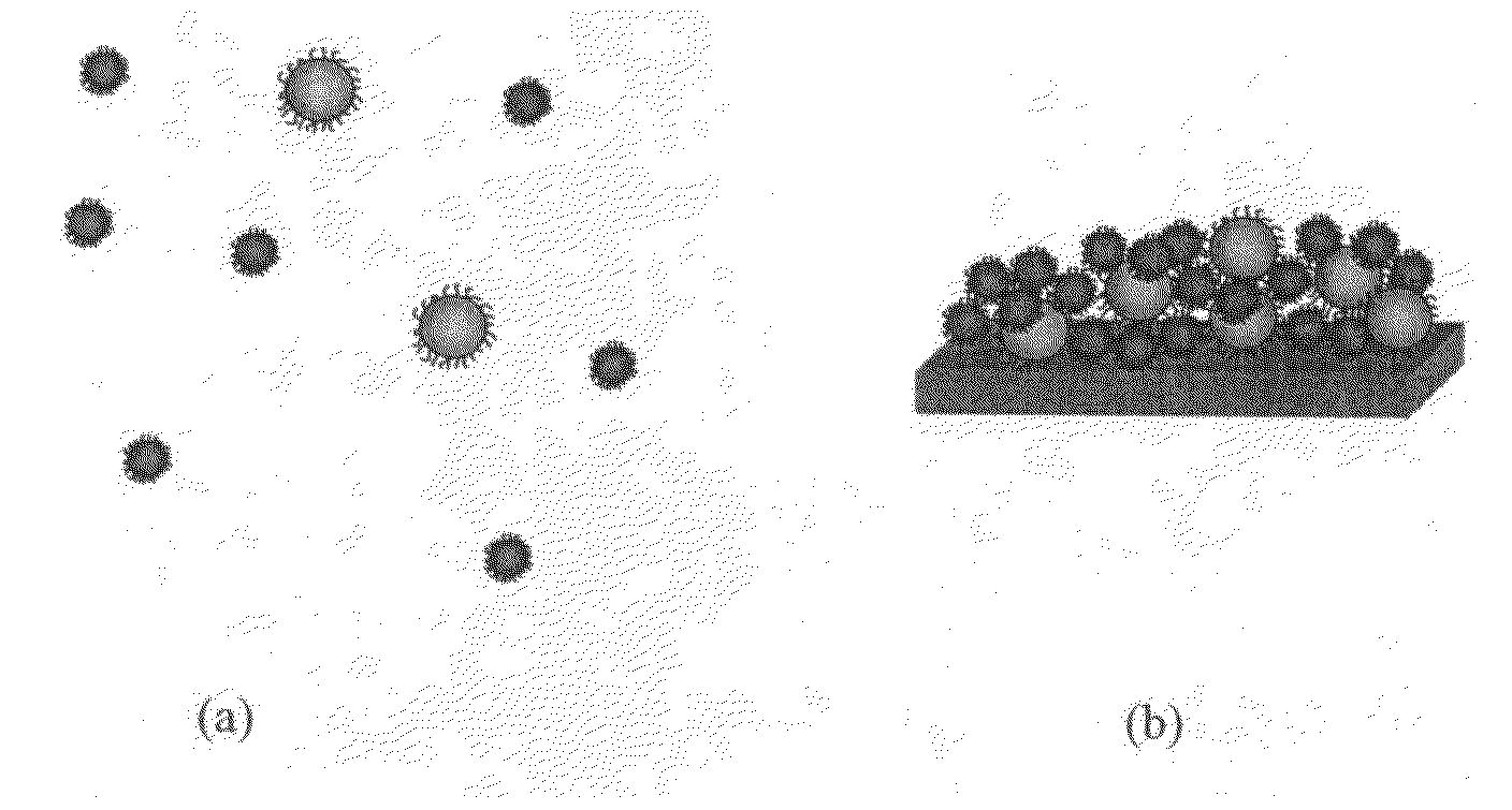
[0011]First, the overall NC density can be maximized giving higher overall film absorbance, electrical conductivity, and emitter density. In previous approaches, NC's would be diluted to increase the distance therebetween, and thus minimize “bad” energy transfer. Another reason for dilution is to reduce reabsorption of emitted photons by either donors or acceptors. In the present invention, absorption occurs both in acceptors and donors; however, emission occurs primarily from acceptors as the ratio of donors to acceptors is optimized, which in turn optimizes energy transfer. Referring to FIG. 1, the small circles represent NC donors whereas the larger circles represent NC acceptors. The present invention allows for a much higher density, or concentration, in a film (FIG. 1b) than in solution (1a). Furthermore, the donors do not reabsorb to any appreciable extent the emission of the acceptors, which allows a high absorption cross-section for the film while avoiding reduced efficiency due to energy transfer and reabsorption. This is particularly important for photoexcited LEEs, and further allows for the production of thick film, high-efficiency LEEs which are necessary for scintillators and color-conversion elements.
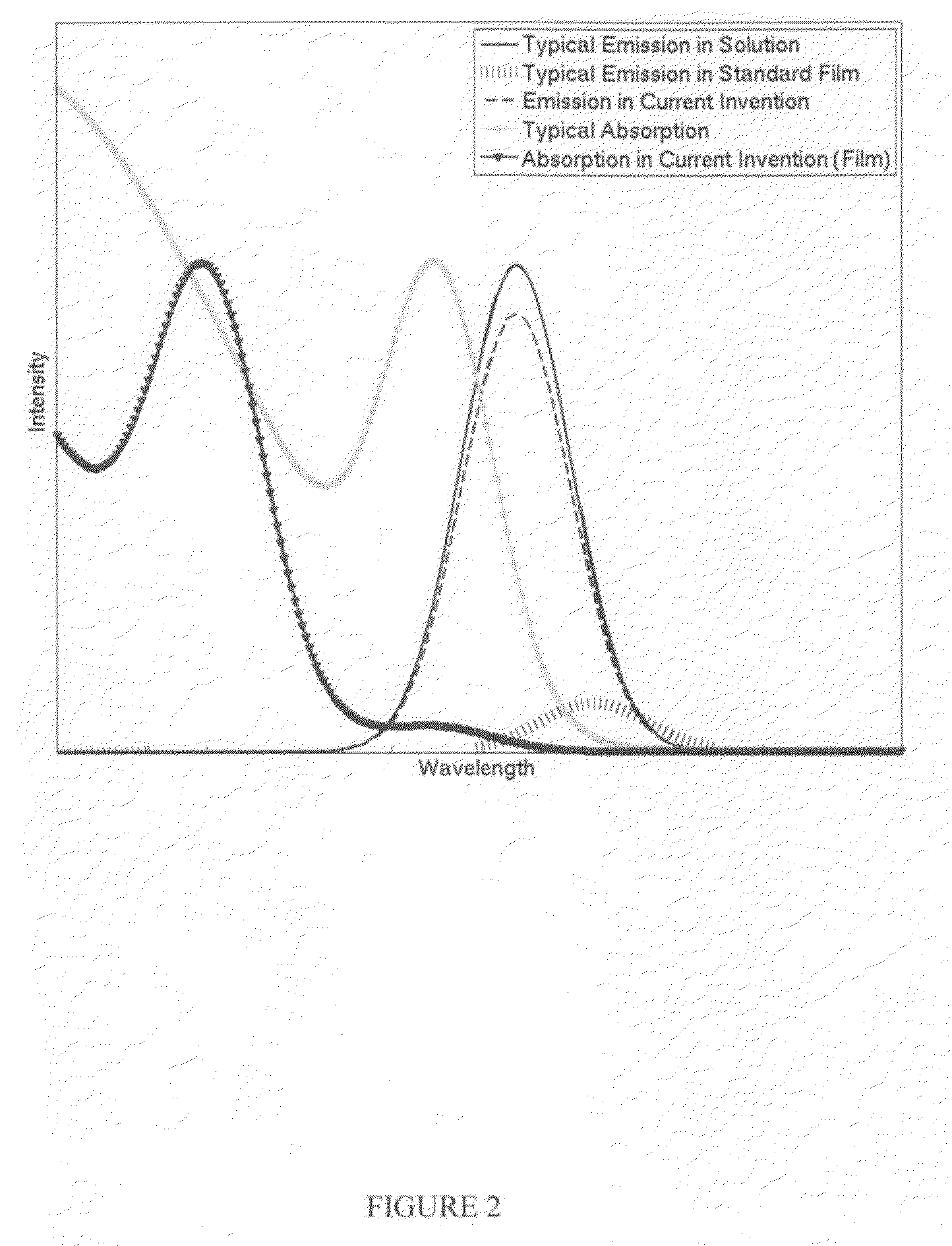
[0012]Second, the emission profile of the solid film device cans be readily controlled to maintain the emission profiles and carrier lifetimes of one or more acceptor NCs in a state similar to that typically only observed in solution-based, or dilute, systems (wherein energy transfer is typically inactive). This prevents emission profiles from being uncontrollably shifted to a longer wavelength (i.e., “red-shifted”) in films relative to solutions. This simplifies the manufacturing control over spectral position and profile, as it is comparable to the solution properties, and also allows for multiple acceptor spectral profiles. A typical dense film of multiple NCs would show efficient energy transfer from the donor NCs indiscriminately to all nearby acceptor NCs of lower band gap energy, resulting in nearly zero emission from the higher band gap NCs and poor control of the resulting spectral profile and position. The current invention circumvents this by using donors which are paired with, or in effect surround, the acceptor NC. The donors serve to funnel energy to the acceptors. This strategy can be used to isolate acceptors from one another, reducing acceptor-acceptor energy transfer, which increases control of the spectral properties of the LEE. For example, a desired emission profile can be produced in solution by mixing multiple NC acceptors to obtain desired emission properties (i.e, a spectral barcode or white-light emission of red, green, and blue nanocrystals) with suitable donors. In the current invention a single film can be used to produce white light. This is simpler than many white light technologies that rely on either red, green, and blue layers or pixels. Films produced via this method will produce a nearly identical spectral profile to the acceptors in solution.
[0013]Third, in the present invention only the acceptors are required to be of high quality. In existing typical NC LEEs, a narrow spectral profile requires the use of highly monodisperse (i.e., nearly identical in size) NCs. This results in higher costs and reproducibility issues. Producing monodisperse, high QY NCs typically requires the production of smaller batches (<10 g) of NCs which also have batch-to-batch variations. The present invention allows the use of low-quality (i.e., poorly size-controlled and correspondingly broad spectral properties), mass-producible, low-cost, and / or lower-toxicity donors, as the emission properties of the donors are unimportant and the donors instead simply absorb and transfer their energy to fewer high-quality (i.e., narrow spectral profile and / or high QY) acceptors. Donors that are produced in larger quantities (>10 g) or through continuous methods where size-control may not be as refined can also be utilized. Acceptors can be produced through various higher-quality synthesis routes yielding high monodispersity and the desired spectral profiles. The resulting mixed films thus potentially offer cost savings, lower toxicity, lower quality-control, and more facile reproducibility.
[0014]Thus, rather than limiting the transfer of energy between nanocrystals, the present invention controls and optimizes energy transfer to increase quantum yield, decrease re-absorption of energy, and increase the control of the spectral properties. The result is a nanocrystal-containing dense film, suitable for use in LEEs, which has the properties of a film (high chromophore density) with the advantages of a solution (high QY and easily controlled spectral properties). Such films, moreover, are useful in photovoltaics for separation of multiple excitons following the generation of multiple excitons from a single photon in a donor NC, and also in optical amplifiers for the generation of multiple excitons (a population inversion) in acceptor NCs. In addition, the compositions of the present invention are useful in other applications in which undesirable energy transfer to or from nanocrystals may have a detrimental effect, for example, in gamma ray detectors, solar cells, and lasers, to name a few.

