

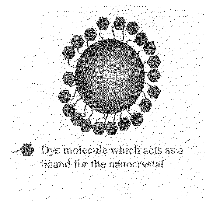
Mixed semiconductor nanocrystal compositions
a semiconductor nanocrystal and composition technology, applied in the field of mixed semiconductor nanocrystal compositions, can solve the problems of loss of emission efficiency, reduced qy, disadvantages of nanocrystal use in lee dense films, etc., and achieves the effects of reducing “bad” energy transfer, reducing qy, and increasing nc density
- Summary
- Abstract
- Description
- Claims
- Application Information
AI Technical Summary
Benefits of technology
Problems solved by technology
Method used
Image

Examples
example 1
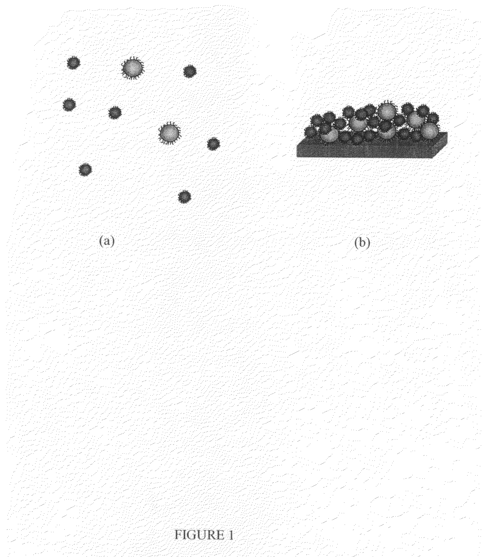
[0048]5 g of 5-nm diameter ZnTe NCs (donors) capped with trioctylphosphine / trioctylphosphine-oxide are dissolved in 25 mL of chloroform. 1 g of 5-nm diameter CdSe NCs (acceptors) capped with trioctylphosphine / trioctylphosphine-oxide and is added to the ZnSe NC solution. 12 g of polymethylmethacrylate (PMMA) is then dissolved in 20 mL of chloroform and added to the mixed-NC solution. The mixture is then poured into a glass form and the solvent is evaporated to produce a solid form. The PMMA helps the solid to retain good optical properties (low scatter) and also causes the NCs to aggregate together such that energy transfer takes place between the donors and acceptors.
example 2
[0049]5 g of polydisperse ZnTe NCs (donors) capped with trioctylphosphine / trioctylphosphine-oxide are dissolved in 25 mL of chloroform. 1 g of 5-nm diameter CdSe NCs (acceptors) capped with trioctylphosphine / trioctylphosphine-oxide and is added to the ZnSe NC solution. The solution is dried and an octane:hexane mixture is returning the solution to the original volume (this allows for high quality drop cast and spin coated films). The resulting mixture is deposited on a GaN LED via spin coating for use as a color conversion element layer.
example 3
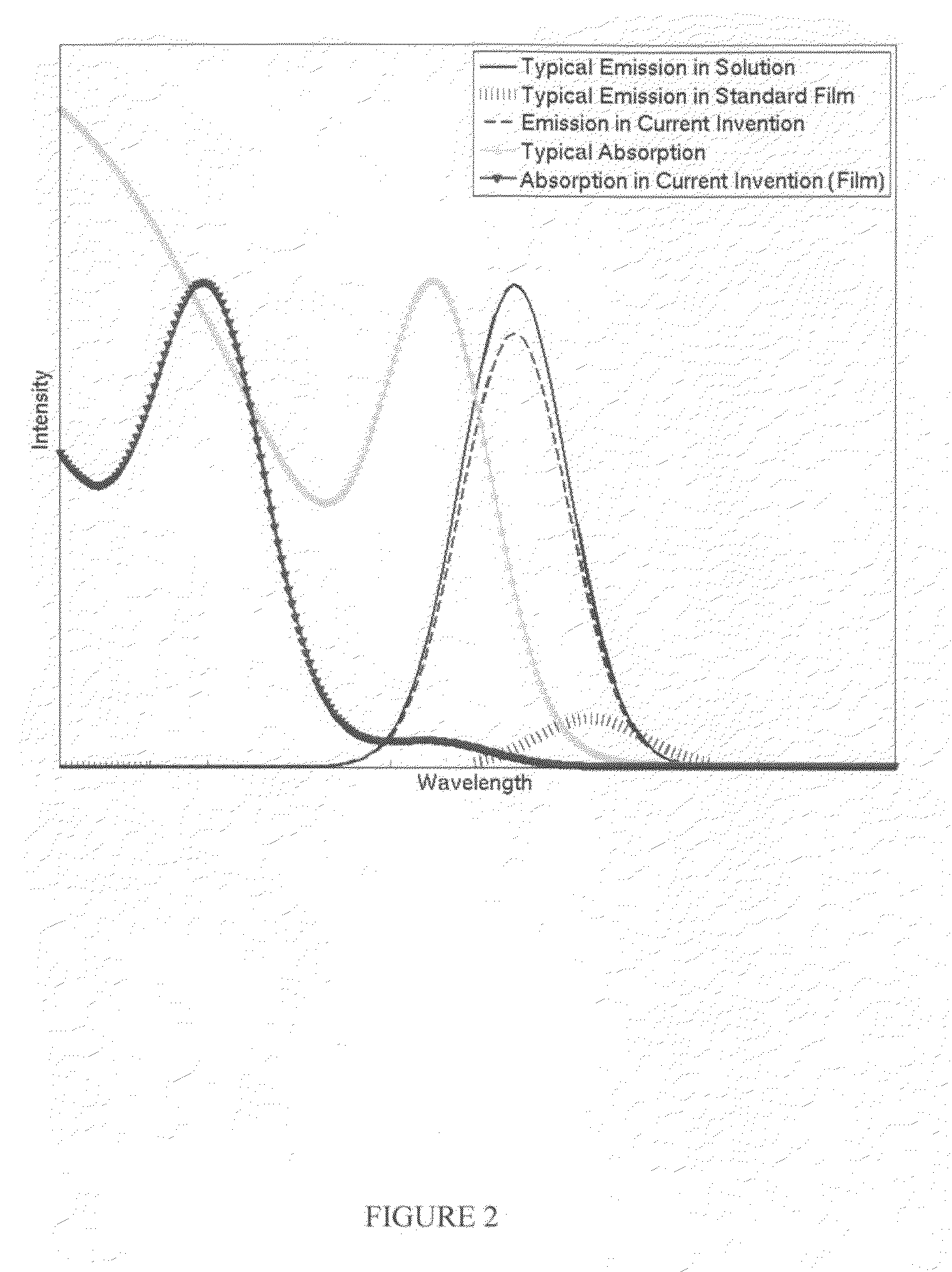
[0050]3 g of 3-nm diameter ZnSe NCs (donors) capped with trioctylphosphine / trioctylphosphine-oxide are dissolved in 30 mL of chloroform. 500 mg of 2.5-nm diameter CdSe NCs (acceptor#1) capped with trioctylphosphine / trioctylphosphine oxide 500 mg of 3.5-nm diameter CdSe NCs (acceptor#2) capped with trioctylphosphine / trioctylphosphine-oxide, and 500 mg of 7-nm diameter CdSe NCs (acceptor#3) capped with trioctylphosphine / trioctylphosphine-oxide are added to the ZnSe NC solution. The mixture stirred and then drop casted onto a glass plate and the solvent is evaporated to produce a solid form. The resulting mixture will have multiple narrow emission peaks from the multiple acceptors and can be tuned to produce white light emission.
PUM
 Abstract
Description
Claims
Application Information