

Nonvolatile semiconductor memory device and control method
a nonvolatile semiconductor and memory device technology, applied in the direction of static storage, digital storage, instruments, etc., can solve problems such as the possibility of program defect states
- Summary
- Abstract
- Description
- Claims
- Application Information
AI Technical Summary
Benefits of technology
Problems solved by technology
Method used
Image



Examples
first embodiment
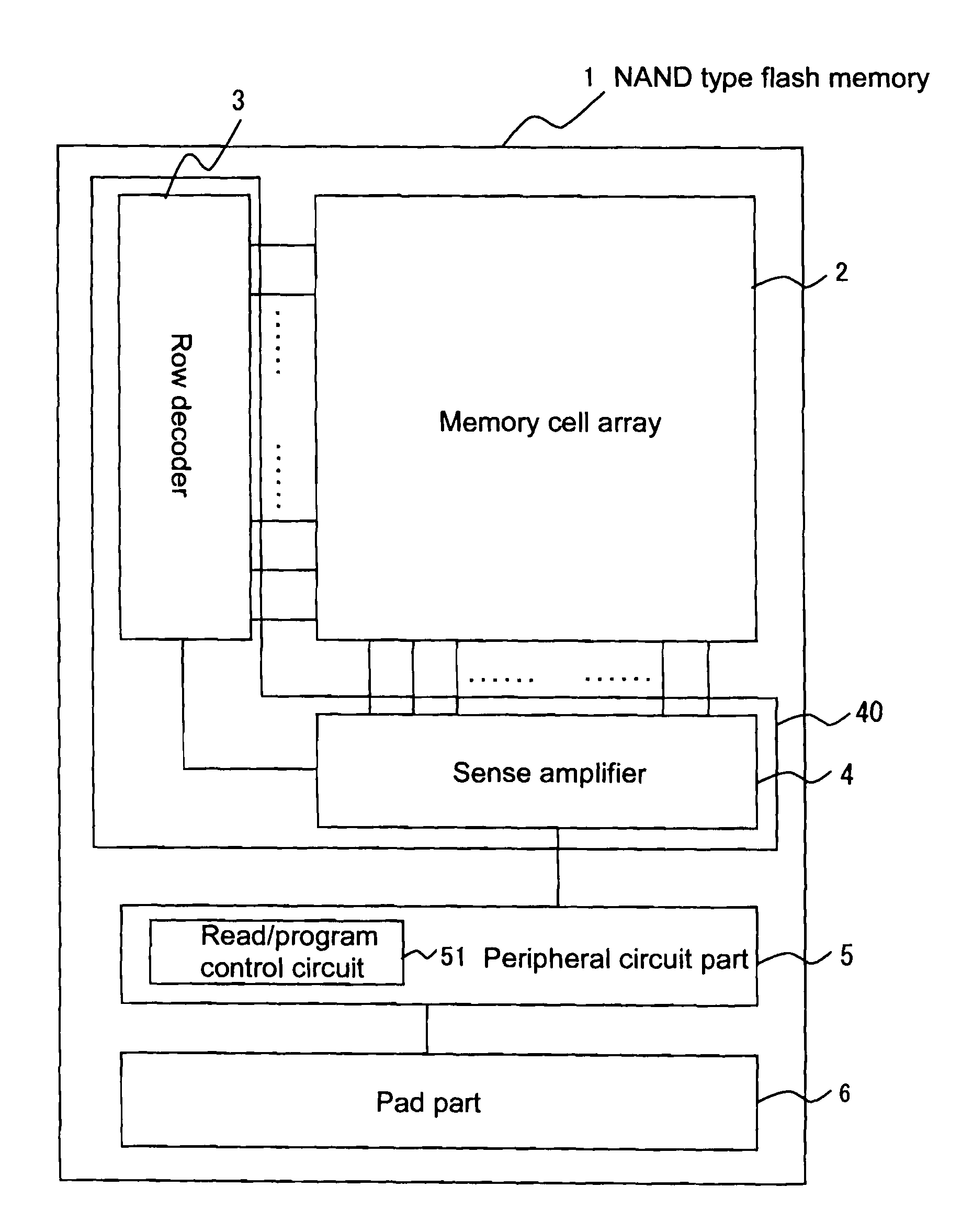
[0027]FIG. 1 is a diagram which shows an outline structure of a NAND type flash memory 1 related to the first embodiment of the present invention. As is shown in FIG. 1, the NAND type flash memory 1 related to the first embodiment of the present invention is arranged with a memory cell array 2, a row decoder 3, a sense amplifier 4, a read / program circuit part 40, a peripheral circuit part 5 and a pad part 6.
[0028]The memory cell array 2 related to the first embodiment includes a plurality of electrically reprogrammable memory cells arranged in a matrix. FIG. 2 is an outline block diagram which shows the structure of the memory cell array 2 related to the first embodiment. The memory cell array 2 includes a plurality (m) of memory cell blocks BLK0, BLK1, . . . , BLKm−1, as is shown in FIG. 2. Here, a memory cell block is the smallest unit in which data can be erased.
[0029]Next, FIG. 3 is a block diagram which shows a more detailed structural example of one memory cell block (for exam...
second embodiment
[0059]In the second embodiment, the case where the NAND type flash memory 1 is programmed with 4 level data will be explained by applying the flowchart of program operations shown in FIG. 6. Furthermore, because the structure of the NAND type flash memory 1 related to the second embodiment is the same as that shown in FIG. 1 to FIG. 4 stated above, a structural explanation will be omitted here.
[0060]A programming operation of 4 level data which is performed to the NAND type flash memory cell 1 related to the second embodiment will be explained while referring to the flowchart shown in FIG. 6 and the transition diagram of a threshold voltage distribution shown in FIG. 8 to FIG. 10. In the flowchart shown in FIG. 6, six types of program verification voltage AVL, AV, BVL, BV, CVL and CV used in program verification control are set as parameters related to program control of the second embodiment to everything shown by the threshold voltage distribution: x=A, B, C (see FIG. 11). The rel...
third embodiment
[0092]In the third embodiment, the case where the NAND type flash memory 1 is programmed with 8 level data will be explained. Furthermore, because the structure of the NAND type flash memory 1 related to the third embodiment is the same as that in FIG. 1 to FIG. 4, a structural explanation will be omitted here.
[0093]A program operation of 8 level data which is performed in the NAND type flash memory 1 of the third embodiment will be explained while referring to the flowchart shown in FIG. 13 and the transition diagram of the threshold voltage distribution shown in FIG. 14 and FIG. 15. In the flowchart shown in FIG. 13, fourteen types of program verification voltages A1VL, A1V, A2VL, A2V, B2VL, B2V, C2VL, C2V, A3V, B3V, D3V, E3V, F3V, G3V used in a program verification control, are set as parameters related to a program control of the third embodiment for everything shown by a threshold voltage distribution: x=A, B, C, D, E, F, G. The relationships between these voltages is A3V2VL2V3...
PUM
 Abstract
Description
Claims
Application Information