Method for designing structured ASICs in silicon processes with three unique masking steps

a technology of structured asics and silicon processes, applied in the direction of pulse techniques, instruments, semiconductor/solid-state device details, etc., can solve the problems of delay and power dissipation of these logic functions, lower performance and/or higher power dissipation of asic devices

Inactive Publication Date: 2011-02-22
BAE SYST INFORMATION & ELECTRONICS SYST INTERGRATION INC
View PDF22 Cites 3 Cited by
  • Summary
  • Abstract
  • Description
  • Claims
  • Application Information

AI Technical Summary

Problems solved by technology

Any delay and power dissipation of these logic functions are caused by the multiplexer and not the actual logic functions.
This results in lower performance and / or higher power dissipation of the ASIC devices.

Method used


Image

  • Method for designing structured ASICs in silicon processes with three unique masking steps
  • Method for designing structured ASICs in silicon processes with three unique masking steps
  • Method for designing structured ASICs in silicon processes with three unique masking steps

Examples


Embodiment Construction

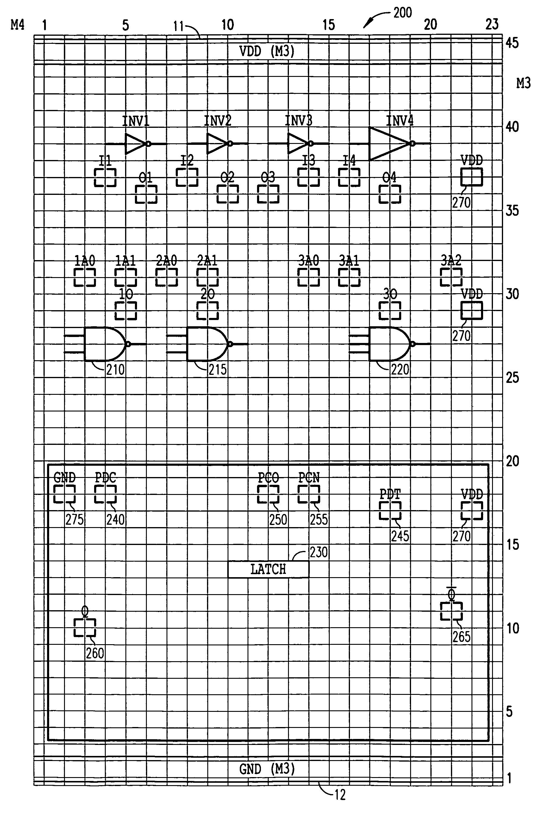
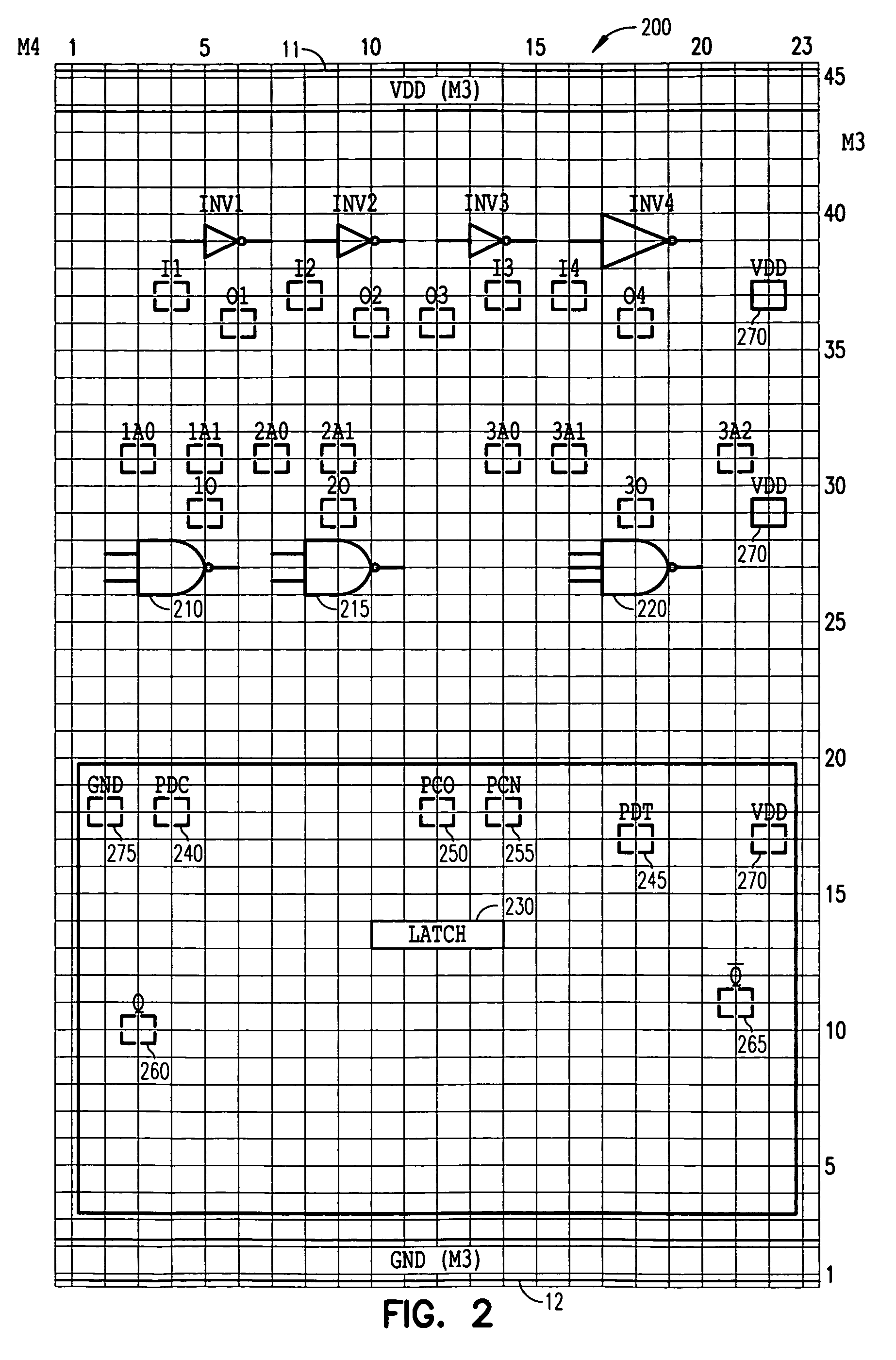
[0012]In the following detailed description, reference is made to the accompanying drawings that show, by way of illustration, specific embodiments in which the invention may be practiced. These embodiments are described in sufficient detail to enable those skilled in the art to practice the invention. It is to be understood that the various embodiments of the invention, although different, are not necessarily mutually exclusive. For example, a particular feature, structure, or characteristic described herein in connection with one embodiment may be implemented within other embodiments without departing from the scope of the invention. In addition, it is to be understood that the location or arrangement of individual elements within each disclosed embodiment may be modified without departing from the scope of the invention. The following detailed description is, therefore, not to be taken in a limiting sense, and the scope of the present invention is defined only by the appended cla...


PUM


Abstract

A multi-function core base cell includes a set of functional microcircuits. These microcircuits are used to design a Library of Logic Function Macros. The functional macros consisting of one or more microcircuits have a fixed and complete physical layout similar to a conventional standard cell library macro set. In addition to a core functional macro set, primary input / output buffers and commonly used single and dual port memory blocks are also defined in the library. The library includes all the ASIC synthesis, simulation, and physical design rules.

Description

CROSS REFERENCE TO RELATED APPLICATIONS[0001]This application claims priority to and is a divisional of application Ser. No. 11 / 147,024 filed Jun. 7, 2005, now U.S. Pat. No. 7,418,692, which issued on Aug. 26, 2008, which in turn claims priority to prior U.S. Provisional Application No. 60 / 578,371, entitled A Method for Designing Structured ASICS in Silicon Processes with Three Unique Masking Steps, filed Jun. 9, 2004, both the patent and the applications are incorporated herein in their entirety for all purposes.TECHNICAL FIELD[0002]Various embodiments of the invention relate to the design and fabrication of application specific integrated circuit (ASIC) devices, and in particular, but not by way of limitation, to a method of ASIC design and fabrication with three unique masking steps per ASIC part.BACKGROUND[0003]A general function ASIC device consists of logic functions such as combinatorial circuits, latches and registers, memory blocks, input / output buffers, and other custom fu...

Claims


Application Information

Patent Timeline
Patent Type & Authority Patents(United States)
IPC IPC(8): G06F17/50G06F17/30
CPCG06F17/5045G06F2217/64G06F30/30G06F2115/06
Inventor BANSAL, JAI P.
Owner BAE SYST INFORMATION & ELECTRONICS SYST INTERGRATION INC
Why Eureka
Try Eureka