Hybrid nanocomposite semiconductor material, and method of producing inorganic semiconductor therefor

a semiconductor material and hybrid technology, applied in the field of hybrid organic/inorganic semiconductor materials and methods of producing inorganic semiconductors therefor, can solve the problems of increasing costs, affecting the efficiency of production, so as to reduce the agglomeration of smaller particles, and reduce the risk of superheating solven

Inactive Publication Date: 2011-03-01
NAT RES COUNCIL OF CANADA
View PDF14 Cites 0 Cited by
  • Summary
  • Abstract
  • Description
  • Claims
  • Application Information

AI Technical Summary

Benefits of technology

[0016]The semiconductor material comprises an inorganic semiconductor incorporated into a film comprising a hole-conductive fluorene copolymer. Advantageously, energy levels (e.g. ionization energy (IP), electro-affinity (EA) and energy gap (Eg)) of both the inorganic semiconductor and the hole-conductive fluorene copolymer may be varied to control and optimize electron hole and conductive pathways thereby increasing power conversion efficiency of the semiconductor material.
[0019]A particularly simple and efficacious method involves mixing inorganic semiconductor precursors with a steric-hindering coordinating solvent, preferably in the absence of surfactant, and heating the mixture with microwaves to a temperature below the boiling point of the solvent. The use of microwaves rather than other energy sources (e.g. ultrasound, convenction, etc.) permits even heating and precise adjustment of reaction temperature to a temperature lower than the boiling point of the solvent thereby reducing the risk of superheating the solvent. Importantly, the use of a steric-hindering coordinating solvent reduces agglomeration of smaller particles into larger aggregates. Particle size may be regulated by controlling reaction time. Reaction times on the order of less than about one minute can result in particles having average diameters of about 2 nm, while reaction times on the order of longer than about ten minutes can result in particles having average diameters of about 6 nm. Average diameter is directly related to heating time. Control of particle size provides the opportunity to tune energy levels in order to optimize photovoltaic properties of the inorganic semiconductor.
[0020]Advantageously, the microwave method can make use of less hazardous starting materials, is more energy efficient, is lower cost, does not require the use of surfactants, requires only one step under ambient conditions, produces little or no waste as recovered solvent and byproducts may be re-used, produces a product mixture that can be directly integrated into active devices, is conducive to large scale preparation, and permits fine tuning of particle size. In addition, this method permits preparation of stable solutions of inorganic semiconductor, which appear resistant to oxygen and moisture and provides luminescent materials when prepared and handles in air. Nanocrystalline particles of inorganic semiconductors having near band-edge photoemission may be prepared.
[0033]Advantageously, it is not necessary to exchange the capping group (e.g. cyclohexanone) with another (e.g. pyridine) since inter-particle separation does not become significantly smaller when compared to trioctylphosphine, therefore, transport properties are not enhanced simply by the exchange of surface functionality as a result of the exchange of capping groups. Annealing the film may improve transport characteristics of the semiconductor material, however, restrictions imposed by the polymer in the semiconductor material prohibit high temperature annealing. Size selective precipitation is also not necessary since in a photovoltaic cell a narrow size distribution is not necessarily beneficial.

Problems solved by technology

For aesthetic and for budgeting reasons, crystalline based solar cells are not the most suitable photovoltaic technology.
For crystalline silicon, the cost of photovoltaic materials and their processing accounts for up to 50% of the total cost of the device.
Since processing crystalline silicon requires the use of high temperature (up to 2000° C. or more) and high vacuum, costs are expected to keep rising.
However, even after several decades of intense R&D the cost of electricity production from solar energy is still about 10 times higher than fossil fuel-based power generation.
However, because of its indirect energy band gap, silicon is not an efficient light absorption material in comparison with direct band gap semiconductors with similar characteristics.
Thus, relatively thick film (several hundred micrometers) of expensive high purity silicon is required to absorb about 90% of impinging solar radiation.
In spite of these advantages, solar energy conversion efficiencies reported so far on organic photovoltaic cells are much lower than the 24% efficiency obtained with mono-crystalline silicon based solar cells.
However, blending has not lead to a significant enhancement in power conversion efficiency.
One of the main bottlenecks is the lack of efficient charge recuperation leading to significant charge recombination.
This limits the efficiency of charge transfer to the electrode.
The low intrinsic carrier mobility of plastic materials is considered to be the main obstacle in achieving high efficiency in organic solar cells.
Although dye sensitized solar cell technology has attracted large interest from both academia and industry, it is still hindered by some stability issues.
However in such photovoltaic materials, the only component that permits tunability is the inorganic semiconductor component.

Method used


Image

  • Hybrid nanocomposite semiconductor material, and method of producing inorganic semiconductor therefor
  • Hybrid nanocomposite semiconductor material, and method of producing inorganic semiconductor therefor
  • Hybrid nanocomposite semiconductor material, and method of producing inorganic semiconductor therefor

Examples


example 1

Preparation of Inorganic Semiconductor Nanoparticles

1A: CdS Nanoparticles

[0055]CdS nanoparticles were prepared using cadmium acetate (Aldrich) and thiourea (Aldrich) as precursors. 50 mL of DMF (Aldrich) in a flask was degassed for 30 minutes under N2. Cadmium acetate (0.0355 g of Cd(OAc)2.H2O) and thiourea (0.0092 g) were combined into the DMF and stirred until the reagents were completely dissolved. The solution was then placed in a microwave equipped with an opening to allow a condenser out of the microwave chamber (Model Mars 5×CEM system with a 2.45 GHz working frequency). Heating temperature and hold time were controlled to provide tunability in particle size distribution. Temperature control was provided with a fibre optic thermocouple placed near the solution. For particles of 5 nm in diameter, the ramp time was 5 minutes, the final temperature was 90° C. and the hold period was 30 minutes. As soon as the hold period was complete, the flask is put into an ice bath with conti...

example 2

Preparation of Thin Films of Semiconductor Material

2A: Films of CdS Embedded in PFOx4:1

[0064]An alternating copolymer of 9,9-dioctylfluorene and oxadiazole having a fluorene:oxadiazole ratio of 4:1 (PFOx4:1) was prepared in accordance with Ding et al. as indicated previously. A solution was prepared containing both PFOx4:1 and the CdS nanoparticles from Example 1A. Thus, PFOx4:1 was dissolved in toluene in a weight concentration of 0.017% or 0.17 g / L. CdS particles were used as prepared in DMF and were present in a concentration of 0.0025M.

[0065]Thin films were prepared by solvent evaporation on glass substrates. The surface of the glass was first rinsed with acetone and allowed to dry. A freshly made solution of PFOx4:1 and CdS was placed on the glass surface until it completely covers it. The so-formed liquid film was then partially covered with a petri dish and placed on a hot plate at a temperature kept lower than 60° C. A thin film of the semiconductor material comprising CdS a...

example 3

Characterization of Inorganic Semiconductor Nanoparticles and Thin Films of Semiconductor Material

Scanning Electron Microscopy (SEM)

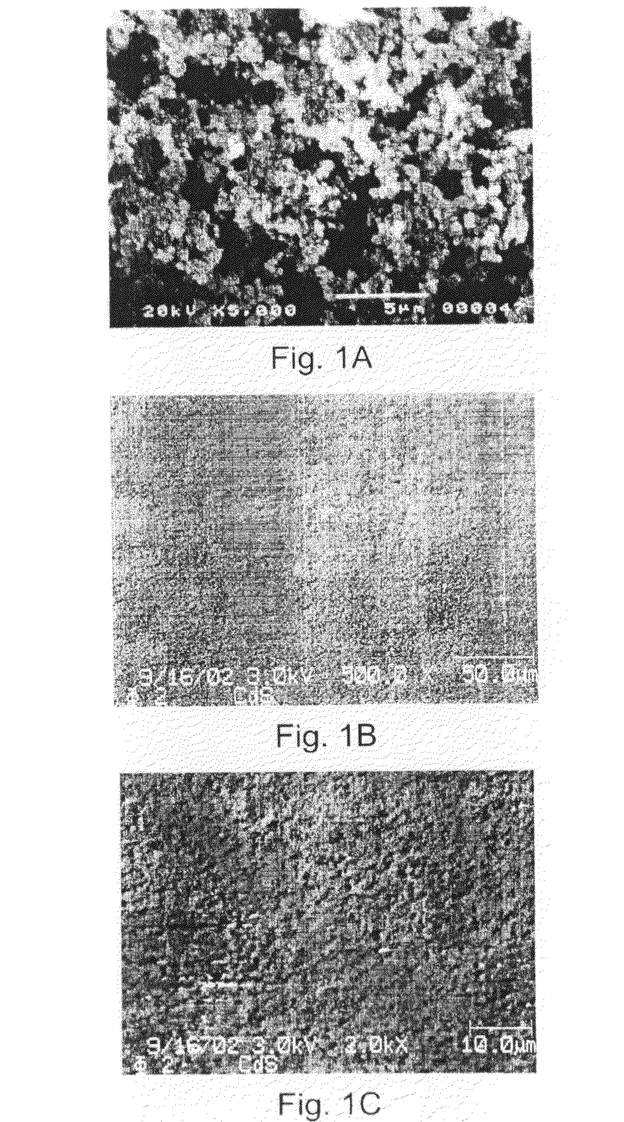
[0067]A scanning electron micrograph (SEM) of CdSe nanoparticles of Example 1B is depicted in FIG. 1A. In three dimensions, the particles appear spherical having a diameter on the order of 50 nm.

[0068]Scanning electron micrographs of a thin film of CdS embedded in PFOx4:1 (FIGS. 1B (500× magnification) and 1C (2000× magnification)) indicate that the film is quite smooth.

Transmission Electron Microscopy (TEM)

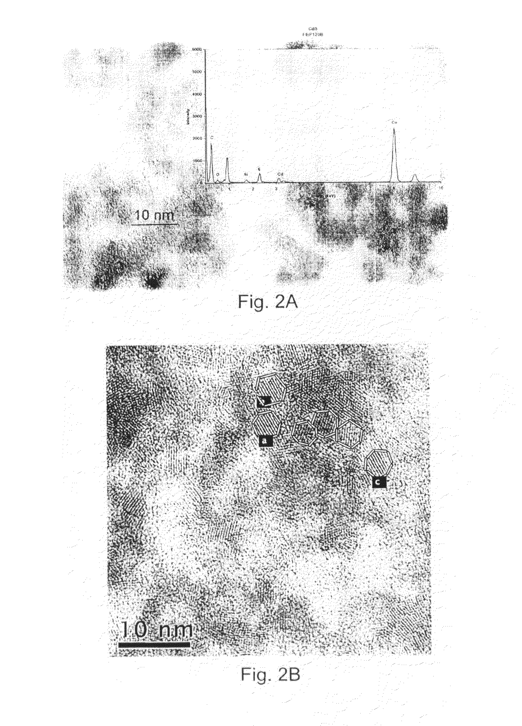
[0069]To prepare samples for TEM, a small amount of each sample was suspended in a solvent (isopropyl alcohol for CdS and acetone for CdSe) and shaken vigorously, for example by sonication. A drop of the resulting suspension was placed on a carbon-coated holey copper grid and dried in air. The dried grid was loaded in a double tilt sample holder. Samples were examined with a Philips CM20 STEM equipped with a Gatan UltraScan 1000 CCD camera, and an en...


PUM

PropertyMeasurementUnit
temperatureaaaaaaaaaa
thickaaaaaaaaaa
energy band-gapaaaaaaaaaa

Abstract

Hybrid semiconductor materials have an inorganic semiconductor incorporated into a hole-conductive fluorene copolymer film. Nanometer-sized particles of the inorganic semiconductor may be prepared by mixing inorganic semiconductor precursors with a steric-hindering coordinating solvent and heating the mixture with microwaves to a temperature below the boiling point of the solvent.

Description

CROSS-REFERENCE APPLICATIONS[0001]This application is a National Stage application of PCT Application PCT / CA2006 / 001112 filed 11 Jul. 2006 which claims benefit of U.S. Provisional Application 60 / 697,532 filed Jul. 11, 2005.FIELD OF THE INVENTION[0002]The present invention is directed to hybrid organic / inorganic semiconductor materials and to methods of producing inorganic semiconductors therefor.BACKGROUND OF THE INVENTION[0003]Since the first report of a semiconductor p-n junction solar cell from Bell Laboratories more than a half a century ago, silicon (amorphous, polycrystalline or monocrystalline) has dominated the photovoltaic market with nearly 99% market share. More than 90% of photovoltaic panels (sold and installed) are based on crystalline (mono and polycrystalline) silicon. For aesthetic and for budgeting reasons, crystalline based solar cells are not the most suitable photovoltaic technology. For this reason, the various thin film-based photovoltaic panels are expected t...

Claims


Application Information

Patent Timeline
Patent Type & Authority Patents(United States)
IPC IPC(8): H01L21/00
CPCB82Y20/00B82Y30/00C09K11/02C09K11/565C09K11/883H01L51/426H01L51/0039H01L51/0587H01L2251/5369Y02E10/549Y10S977/834Y10S977/815Y10S977/823Y10S977/817H10K85/115H10K10/29H10K30/35H10K2102/331
Inventor BENSEBAA, FARIDL'ECUYER, PASCALDING, JIANFUFIRTH, ANDREA
Owner NAT RES COUNCIL OF CANADA
Why Eureka
Try Eureka