Light emitting device and manufacturing method thereof

a technology of light emitting devices and manufacturing methods, applied in the direction of solid-state devices, semiconductor devices, thermoelectric devices, etc., can solve the problems of high film resistance of transparent electrodes and restricted opening ratios

Inactive Publication Date: 2011-03-01
SEMICON ENERGY LAB CO LTD
View PDF178 Cites 31 Cited by
  • Summary
  • Abstract
  • Description
  • Claims
  • Application Information

AI Technical Summary

Benefits of technology

[0013]A problem of the top emission structure is that its transparent electrode has high film resistance. The film resistance becomes even higher when the thickness of the transparent electrode is reduced. When the transparent electrode that serves as a cathode (or an anode) is high in film resistance, a voltage drop makes the intra-plane electric potential distribution uneven and the luminance becomes fluctuated among light emitting elements. Another object of the present invention is therefore to provide a light emitting device structured so as to lower the film resistance of a transparent electrode in a light emitting element, as well as a method of manufacturing the light emitting device. Still another object of the present invention is to provide an electric appliance that uses this light emitting device as its display unit.
[0015]In the present invention, emitted light in the lateral direction is reflected or collected at an inclined surface formed in the first electrode to increase the amount of emitted light taken out in one direction (direction passing through the second electrode).
[0018]Further, the inclined surface formed in the first electrode prevents emitted light from the light emission device (also including emitted light in the lateral direction) from reaching a TFT.
[0038]Further, in accordance with the invention, the shape of an insulator (referred to bank, partition wall, barrier wall, etc.) disposed between each of pixels is improved for eliminating coverage failure, etc. upon forming an layer containing an organic compound layer comprising a polymeric material by a coating method. In each of the constitutions described above, the upper end of the insulator is provided with a curved surface having a radius of curvature, and the radius of curvature is from 0.2 μm to 3 μm. Further, the tapered angle for the insulator may be 35° to 70°.
[0039]By the provision of the radius of curvature, the step coverage is enhanced and a layer containing an organic compound to be formed subsequently can be formed even when it is extremely thin.

Problems solved by technology

There has been a problem in the structure that an opening ratio is restricted depending on an arrangement of TFT and wirings in a pixel portion when definition is to be improved.
For example, light emitted in the lateral direction (the direction parallel to the substrate face) is not taken out and therefore is a loss.
A problem of the top emission structure is that its transparent electrode has high film resistance.

Method used


Image

  • Light emitting device and manufacturing method thereof
  • Light emitting device and manufacturing method thereof
  • Light emitting device and manufacturing method thereof

Examples


embodiment mode 2

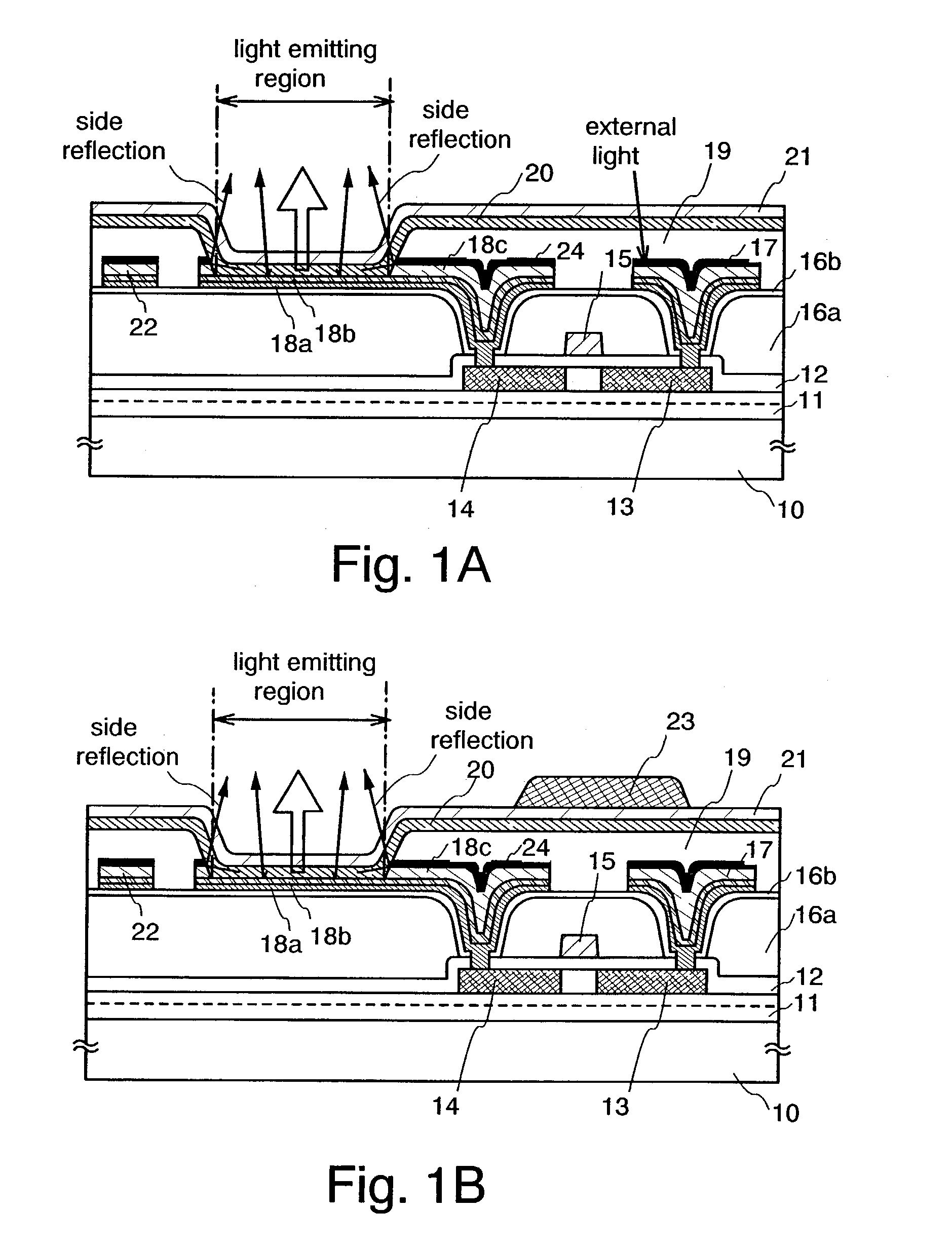
[0116]A method of combining a white color luminescent element and a color filter (hereinafter, referred to as color filter method) will be explained in reference to FIG. 5A as follows.

[0117]The color filter method is a system of forming a light emitting element having an layer containing an organic compound layer displaying white color luminescence and passing the provided white color luminescence through a color filter to thereby achieve luminescence of red, green, and blue.

[0118]Although there are various methods of achieving white color luminescence, a case of using a luminescent layer comprising a high molecular material formable by coating will be explained here. In this case, doping of a color pigment to the high molecular material for constituting a luminescent layer can be carried out by preparing a solution and can extremely easily be achieved in comparison with a vapor deposition method for carrying out common vapor deposition for doping a plurality of color pigments.

[0119...

embodiment mode 3

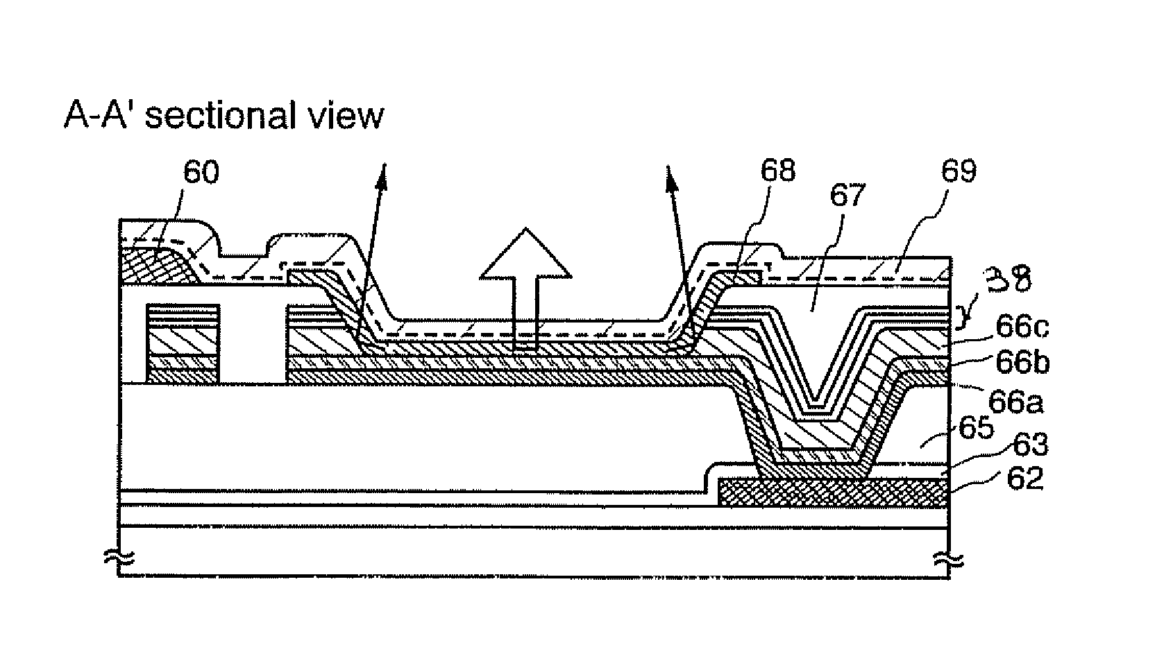
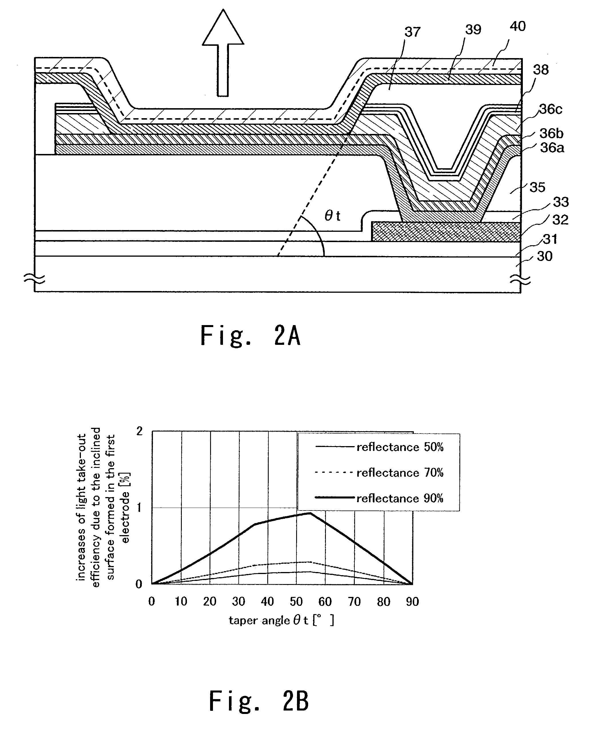
[0133]Other example of the structure is to be described with reference to FIG. 4. Since the embodiment in FIG. 4 is identical with the embodiment of FIG. 2 except for a certain portion, identical portions carry same reference numerals.

[0134]In FIG. 4, after laminating a titanium nitride film 40 on a titanium film 36a to a thickness slightly larger than that of FIG. 2, a portion of the titanium nitride film 40 is also formed as an inclined surface by etching. Since other structures are identical with those in FIG. 2, detailed descriptions of them will be omitted.

[0135]Further, this embodiment mode can be optionally combined with Embodiment Mode 1 or Embodiment Mode 2.

[0136]The present invention comprising the foregoing constitutions is to be described more specifically with reference to examples described below.

embodiment 1

[0137]In this embodiment, a brief description is given with reference to FIGS. 2A to 3C on an example of procedure of forming a light emitting element in accordance with the present invention.

[0138]First, a base insulating film 31 is formed on a substrate 30 which has an insulating surface.

[0139]The base insulating film 31 is a laminate and the first layer is a silicon oxynitride film formed to have a thickness of 10 to 200 nm (preferably 50 to 100 nm) by plasma CVD using as reaction gas SiH4, NH3, and N2O. Here, a silicon oxynitride film (composition ratio: Si=32%, O=27%, N=24%, H=17%) with a thickness of 50 nm is formed. The second layer of the base insulating film is a silicon oxynitride film formed to have a thickness of 50 to 200 nm (preferably 100 to 150 nm) by plasma CVD using as reaction gas SiH4 and N2O. Here, a silicon oxynitride film (composition ratio: Si=32%, O=59%, N=7%, H=2%) with a thickness of 100 nm is formed. Although the base insulating film 108 in this embodimen...


PUM


Abstract

A light emission device manufactured by a method of forming a curved surface having a radius of curvature to the upper end of an insulator 19, exposing a portion of the first electrode 18c to form an inclined surface in accordance with the curved surface, and applying etching so as to expose the first electrode 18b in a region to form a light emission region, in which emitted light from the layer containing the organic compound 20 is reflected on the inclined surface of the first electrode 18c to increase the total take-out amount of light in the direction of an arrow shown in FIG. 1A and, further, forming a light absorbing multi-layered film 24 comprising light absorbing multi-layered film on the first electrode 18c other than the region to form the light emission region, thereby obtaining a light emission device of a structure increasing the amount of light emission taken out in one direction in a light emission element, while not all the light formed in the layer containing the organic compound are taken out from the cathode as a transparent electrode toward TFT but the light was emitted also, for example, in the lateral direction (direction parallel with the plane of the substrate).

Description

BACKGROUND OF THE INVENTION[0001]1. Field of the Invention[0002]The present invention relates to a light emitting device with a light emitting element that emits fluorescent light or phosphorescent light upon application of electric field to a pair of electrodes of the element which sandwich a layer containing an organic compound, and to a method of manufacturing the light emitting device. In this specification, the term light emitting device includes an image display device, a light emitting device and a light source (including illuminating device). Also, the following modules are included in the definition of the light emitting device: a module obtained by attaching to a light emitting device a connector such as an FPC (flexible printed circuit; terminal portion), a TAB (tape automated bonding) tape, or a TCP (tape carrier package); a module in which a printed wiring board is provided at an end of the TAB tape or the TCP; and a module in which an IC (integrated circuit) is directl...

Claims


Application Information

Patent Timeline
Patent Type & Authority Patents(United States)
IPC IPC(8): H01L29/04H01L27/32H01L51/52
CPCH01L27/3244H01L51/5284H01L51/5203H01L51/56H01L51/5271H01L27/3246H01L51/5206H01L2251/56H10K59/122H10K59/12H10K50/813H10K50/818H10K50/856H10K50/865H10K71/00H10K50/805H10K50/81
Inventor YAMAZAKI, SHUNPEINODA, TAKESHIHIGAKI, YOSHINARI
Owner SEMICON ENERGY LAB CO LTD
Why Eureka
Try Eureka