Write assist circuit for improving write margins of SRAM cells

a technology of assist circuit and sram cell, which is applied in the field of memory array and the design and operation of static random access memory array (sram) array, can solve the problems of reducing the speed of write operations, reducing and reducing the resistance of respective read and write operations. , to achieve the effect of improving the vccmin of sram cells and improving the writing speed

Active Publication Date: 2011-03-01
TAIWAN SEMICON MFG CO LTD
View PDF10 Cites 21 Cited by
  • Summary
  • Abstract
  • Description
  • Claims
  • Application Information

AI Technical Summary

Benefits of technology

[0013]The advantageous features of the present invention include increased Vccmin of SRAM cells, and improved writing speed.

Problems solved by technology

Due to the existence of static noise, the reduced read and write margins may cause errors in the respective read and write operations.
In very small-scale integrated circuits, the differential bit-lines BL and BL_ are very thin and narrow, and hence their resistances are no longer negligible.
This may reduce the speed of write operations, and may even cause the failure of the write operations when the write margin reduces to 0 mV.

Method used


Image

  • Write assist circuit for improving write margins of SRAM cells
  • Write assist circuit for improving write margins of SRAM cells
  • Write assist circuit for improving write margins of SRAM cells

Examples


Embodiment Construction

[0022]The making and using of the presently preferred embodiments are discussed in detail below. It should be appreciated, however, that the present invention provides many applicable inventive concepts that can be embodied in a wide variety of specific contexts. The specific embodiments discussed are merely illustrative of specific ways to make and use the invention, and do not limit the scope of the invention.

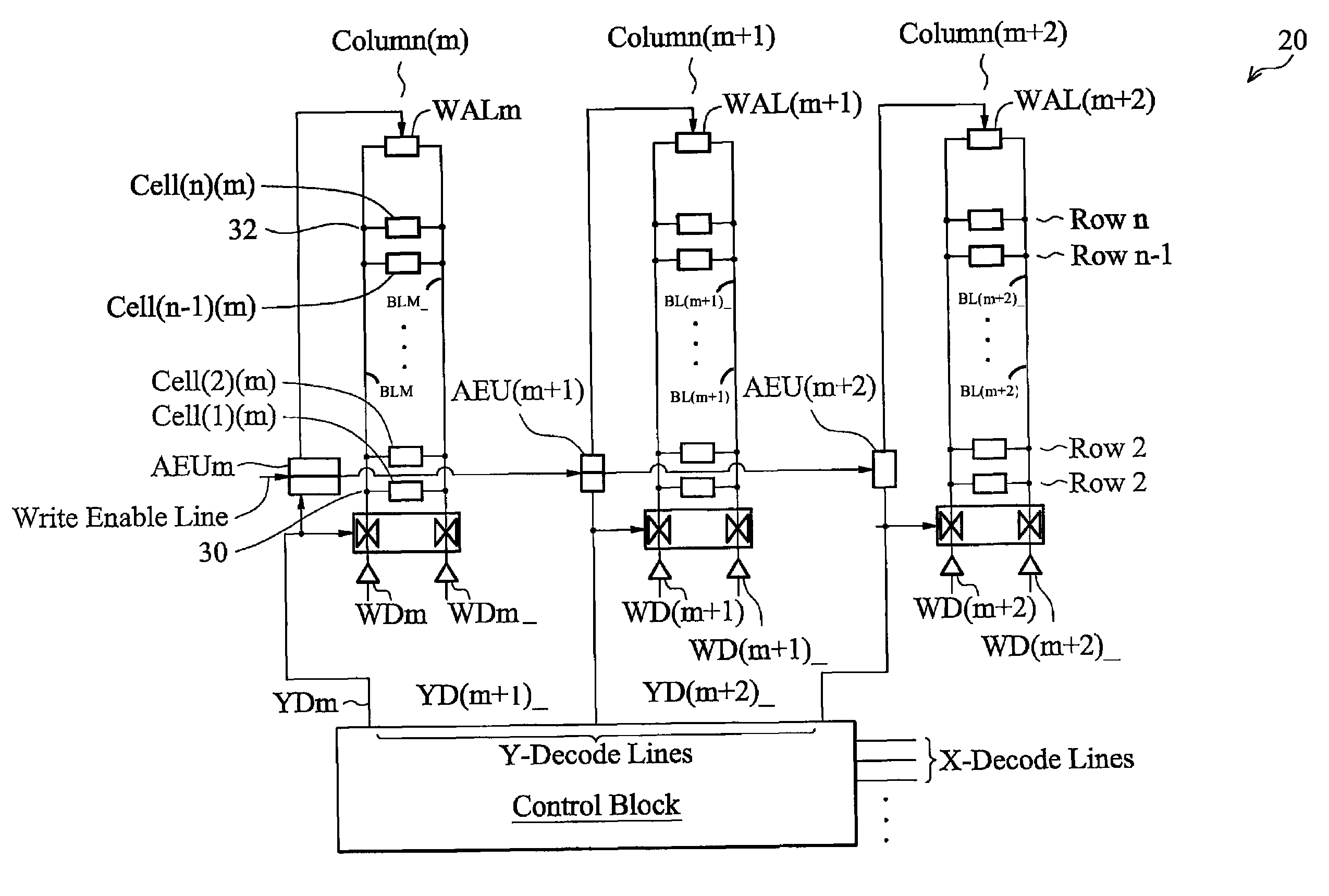
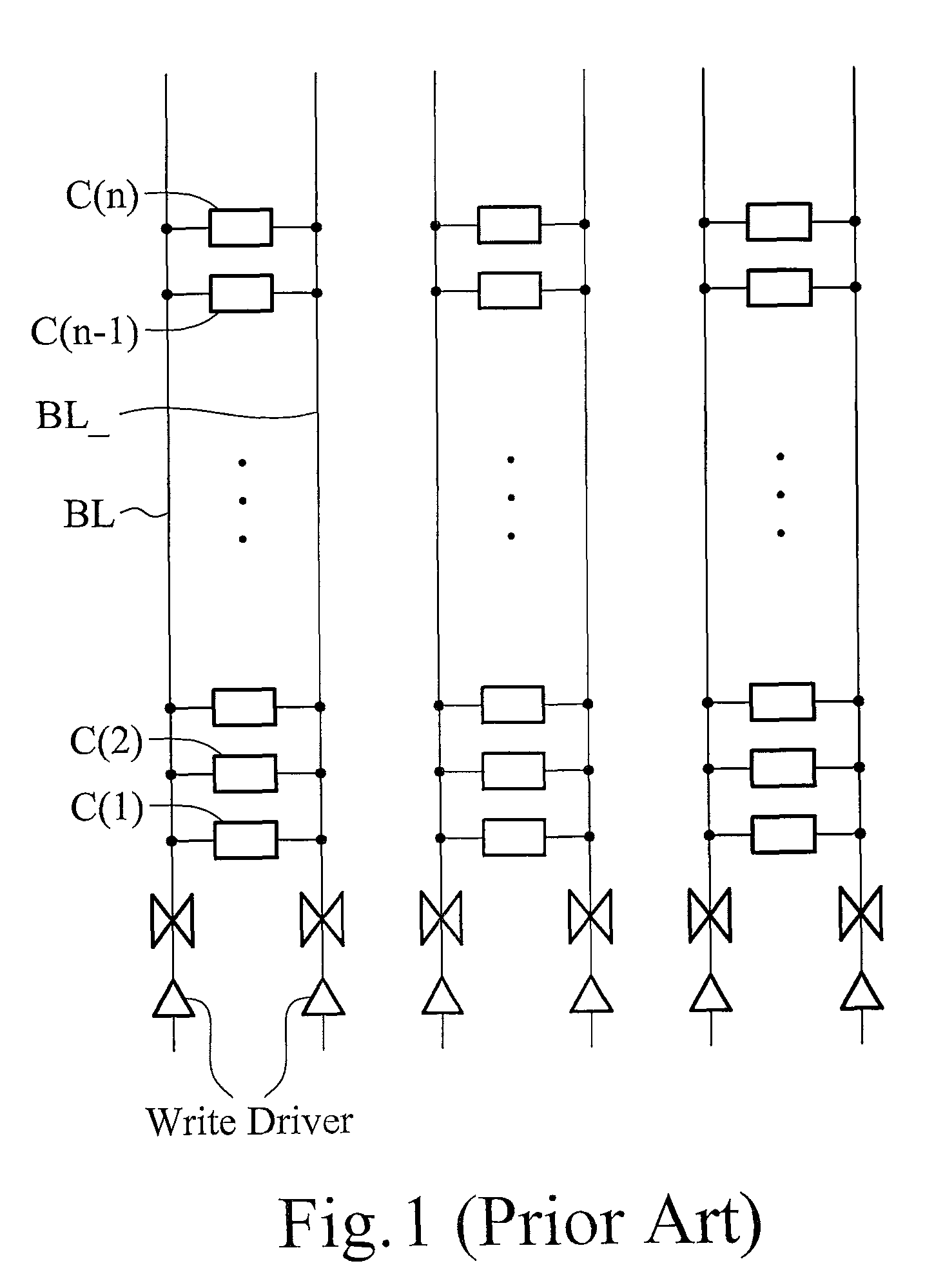
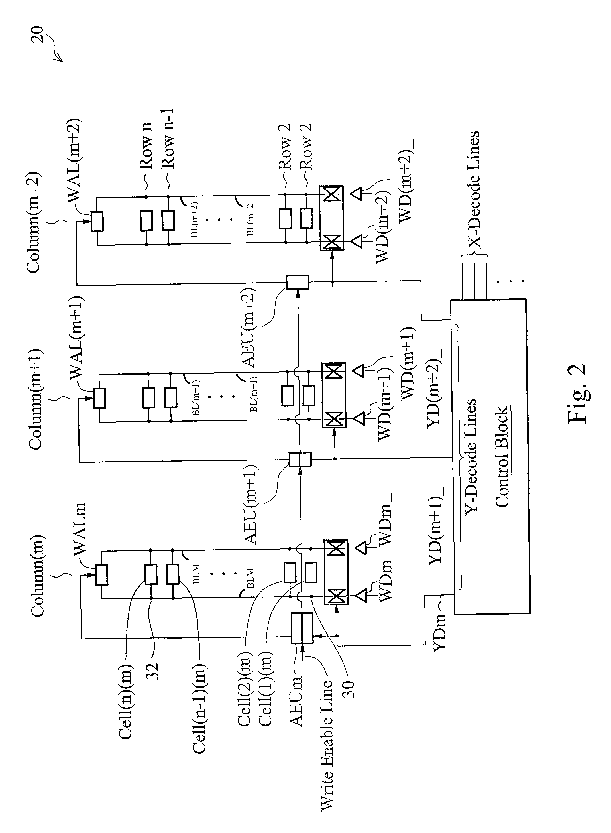
[0023]A novel static random access memory (SRAM) array with improved immunity to the voltage drop on bit-lines is provided. The variations and operations of the preferred embodiments are then discussed. Throughout the various views and illustrative embodiments of the present invention, like reference numbers are used to designate like elements.

[0024]FIG. 2 illustrates an embodiment of the present invention, wherein a portion of SRAM array 20 is shown. SRAM array 20 includes a plurality of rows and a plurality of columns. FIG. 2 only illustrates columns m, m+1, and m+2, where ...


PUM


Abstract

A memory circuit includes a memory array, which further includes a plurality of memory cells arranged in rows and columns; a plurality of first bit-lines, each connected to a column of the memory array; and a plurality of write-assist latches, each connected to one of the plurality of first bit-lines. Each of the plurality of write-assist latches is configured to increase a voltage on a connecting one of the plurality of first bit-lines.

Description

[0001]This application claims priority to U.S. Provisional Patent Application Ser. No. 61 / 127,585, filed May 14, 2008, and entitled “Write Assist Circuit for Improving Write Margins of SRAM Cells,” which application is hereby incorporated herein by reference.TECHNICAL FIELD[0002]This invention relates generally to semiconductor devices, and more particularly to memory arrays, and even more particularly to the design and operations of static random access memory (SRAM) arrays.BACKGROUND[0003]Static random access memory (SRAM) is commonly used in integrated circuits. SRAM cells have the advantageous feature of holding data without a need for refreshing. SRAM cells may include different numbers of transistors, and are often accordingly referred to by the number of transistors, for example, six-transistor (6T) SRAM, eight-transistor (8T) SRAM, and the like. The transistors typically form a data latch for storing a bit. Additional transistors may be added to control the access to the tra...

Claims


Application Information

Patent Timeline
Patent Type & Authority Patents(United States)
IPC IPC(8): G11C7/10
CPCG11C11/413
Inventor TAO, DEREK C.LUM, ANNIE-LI-KEOWLU, CHUNG-JIKENGERI, SUBRAMANI
Owner TAIWAN SEMICON MFG CO LTD
Why Eureka
Try Eureka