
LED light source device

a light source device and led light technology, applied in semiconductor devices for light sources, lighting and heating apparatus, planar/plate-like light guides, etc., can solve the problems of difficult design production, high light utilization factor cannot be achieved, and it is difficult for irradiation to be conducted in a uniform manner on this irradiated surface at a high illuminance, so as to prevent the occurrence of boundary reflection, easy to control the distribution, and high degree of design freedom

Active Publication Date: 2011-03-08
USHIO DENKI KK
View PDF18 Cites 27 Cited by
  • Summary
  • Abstract
  • Description
  • Claims
  • Application Information

AI Technical Summary

Benefits of technology

The solution achieves high light utilization efficiency and uniform irradiation with high illuminance on large surfaces, eliminating the need for multiple LED packages and reducing design complexity.

Problems solved by technology

As a result, a high factor of light utilization cannot be achieved.
Moreover, for the sake of achieving a favorable form of radiated light, it is necessary to create designs that take into consideration these instances of refraction at the boundary surfaces, and the problem is that such designs themselves are difficult to produce.
Because of this, a problem exists in which it is difficult for irradiation to be conducted in a uniform manner on this irradiated surface at a high illuminance.
Therefore, this type of LED light source device is not suitable for light irradiation of surfaces that have a considerable amount of surface area.
That is to say, in order to provide light irradiation on a surface that has a broad surface area, several LED packages composed of luminescent elements and optical members must be provided, and even in cases where the configuration is such that these multiple LED packages are arranged on a common substrate, it is impossible to conduct even irradiation of light onto the surface, and moreover, it is impossible to obtain a sufficient illuminance in order to do so.

Method used


Image

  • LED light source device
  • LED light source device
  • LED light source device

Examples


Embodiment Construction

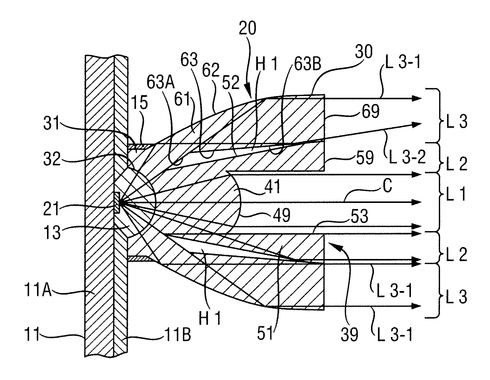
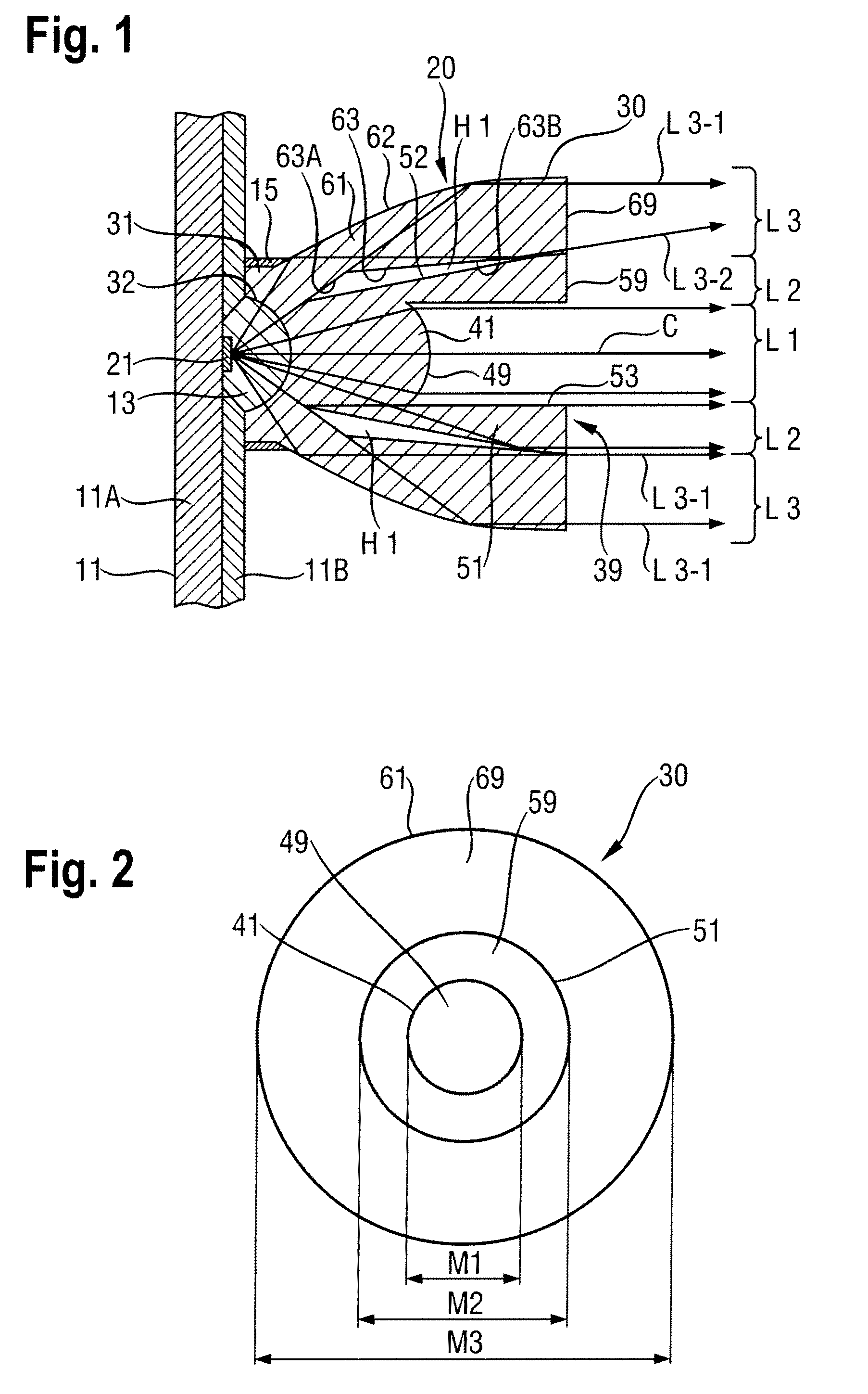
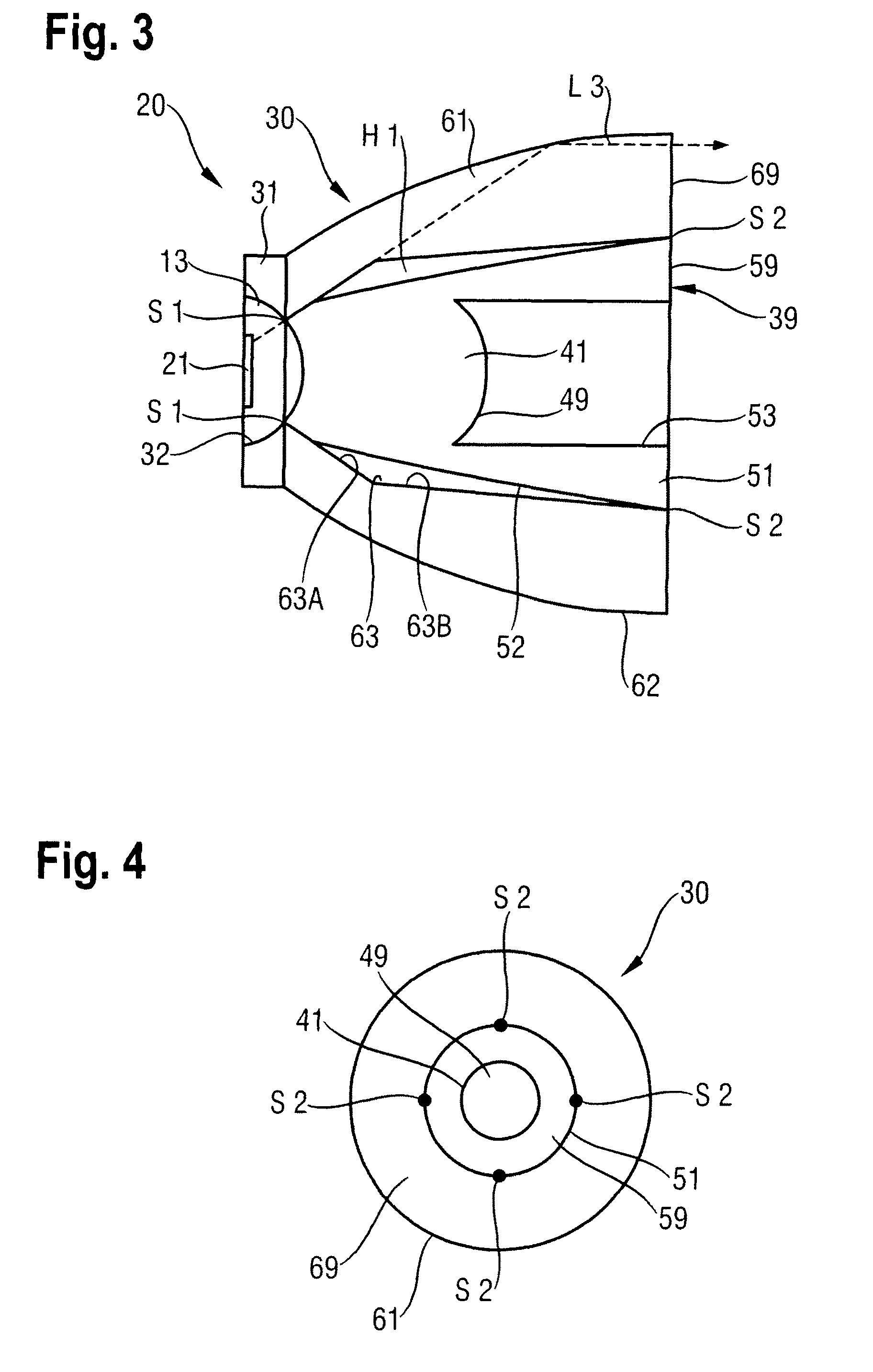
[0032]The LED light source device of the invention is equipped with luminescent elements (LED: Light-Emitting Diode) 21 that are used as a light source, and the LED package 20 that is made up of these elements 21 along with a translucent light-guiding member 30 that is used as an optical member are installed onto a substrate 11.

[0033]The luminescent elements 21 that make up the LED package 20 are arranged such that an insulation layer 11B is laminated onto the base material 11A, followed by a wire pattern (not shown) that is formed on this insulation layer 11B to form the substrate 11, onto which the luminescent elements 21 are placed in their positions that are exposed on the base material 11A, after which they are electrically connected to the wiring pattern that is formed on the insulation layer 11B.

[0034]In the example shown in FIG. 1, the luminescent elements 21 are molded using a hemispherical molding member 13 in which a heat-resistant translucent resin such as a silicon resi...


PUM


Abstract

An LED light source device using light from luminescent elements at a high level of uniformity and efficiency, and to conduct irradiation with a high level of design freedom an LED light source device is equipped with luminescent elements and a translucent light-guiding member. The translucent light-guiding member has a central convex lens with a first cylindrical light-guiding part formed on the outer periphery of the central convex lens and a second cylindrical light-guiding part formed on the outer periphery of the first cylindrical light-guiding part, such that an air layer is formed between the outer peripheral surface of the first cylindrical light-guiding part and the inner peripheral surface of the second cylindrical light-guiding part, the outer peripheral surface of the first cylindrical light-guiding part and the outer peripheral surface of the second cylindrical light-guiding part being rotated quadratic surfaces with the same focal point.

Description

BACKGROUND OF THE INVENTION[0001]1. Field of Invention[0002]The present invention relates to an LED light source device, and more specifically, an LED light source device in which light from an LED (Light-Emitting Diode) is emitted in a specified direction and within a certain range via an optical member.[0003]2. Description of Related Art[0004]Conventionally, luminescent elements (LEDs) are used as a light source, an optical member is used such as a lens so that the light from this light source is radiated in a specific direction, and an LED light source device is widely used in order to control the light distribution from this optical member. (For an example, refer to published Japanese Patent Application No. H08 (1996)-107235.)[0005]In order to effectively make use of light from luminescent elements (LEDs) used as a light source in an LED light source device of this constitution, a configuration is presented whereby a reflecting mirror is provided in order to cause the portion of...

Claims


Application Information

Patent Timeline
Patent Type & Authority Patents(United States)
IPC IPC(8): F21V1/00H01L33/48H01L33/58H01L33/60
CPCG02B6/0018H01L33/58F21K9/00Y10S362/80G02B6/002F21K9/69
Inventor KABUKI, KIYOYUKIHATA, HIROSHIGE
Owner USHIO DENKI KK
Learn More