Semiconductor package and method for manufacturing the same

a technology of semiconductors and packaging, applied in the field of semiconductor packaging, can solve the problems of thin-type substrate warping and serious warping of bga packages having thin-type substrates during subsequent thermal processes, and achieve the effect of decreasing the processing step of semiconductor packages

Active Publication Date: 2011-03-08
ADVANCED SEMICON ENG INC
View PDF3 Cites 7 Cited by
  • Summary
  • Abstract
  • Description
  • Claims
  • Application Information

AI Technical Summary

Benefits of technology

[0012]It is an object of the present invention to provide a semiconductor package, wherein the mechanical robustness of a stiffener that can prevent a carrier (e.g. substrate) from warping during subsequent thermal processes. Also, the stiffener can be directly mounted on the carrier by the attaching force of an encapsulant. It is not necessary that the stiffener is attached on the carrier by an extra adhesive, thereby decreasing the processing step of the semiconductor package.
[0014]The stiffener includes metal or any other solid material which has an enough mechanically robustness. The height of the stiffener of the present invention can be smaller than that of the chip, and the enough mechanical robustness of the stiffener that can prevent the carrier (e.g. substrate) from warping during subsequent thermal processes. Compared with the prior art, the height of the stiffener of the present invention is smaller than that of the chip so as to cause the stiffener of the present invention to have smaller volume. Thus, the stiffener of the present invention is more economical, and is easily sawed. Furthermore, the stiffener can include a groove adjacent to the carrier. The groove can increase an attaching area (i.e. an attaching force) between the encapsulant and the stiffener so as to directly mount the stiffener on the carrier. In addition, the stiffener of the present invention can be directly mounted on the carrier by the attaching force of the encapsulant. It is not necessary that the stiffener of the present invention is attached on the carrier by an extra adhesive, thereby decreasing the processing step of the semiconductor package.

Problems solved by technology

However, a thin type substrate has a problem of warping.
Due to the different CTE's of various conductive and insulating materials used in the BGA package after the BGA package is packaged, the BGA package having the thin type substrate may be warped seriously during subsequent thermal processes (e.g. a reflow process).
The warping of the BGA package may cause the substrate not to be co-plane so as to further have a problem of solder ball joints.

Method used


Image

  • Semiconductor package and method for manufacturing the same
  • Semiconductor package and method for manufacturing the same
  • Semiconductor package and method for manufacturing the same

Examples


Embodiment Construction

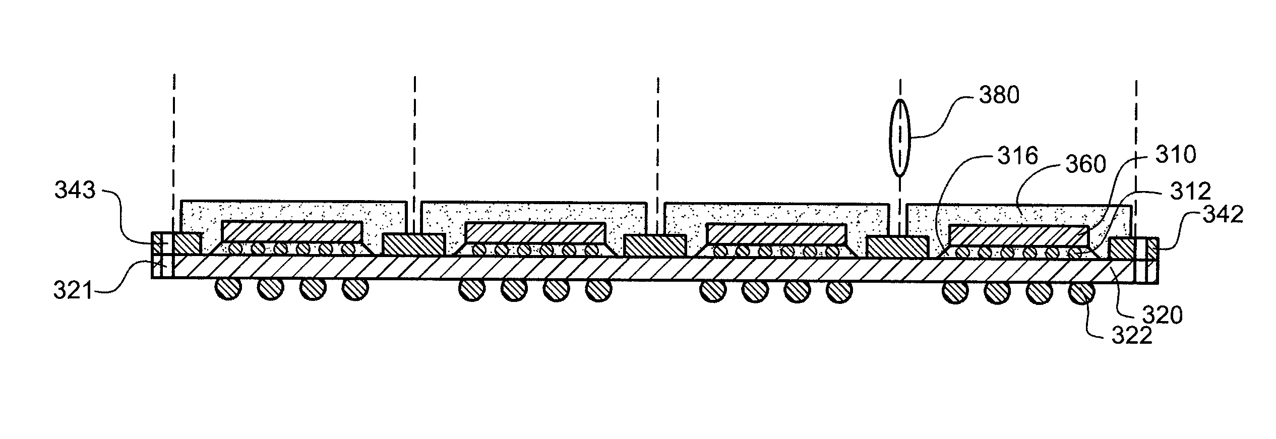
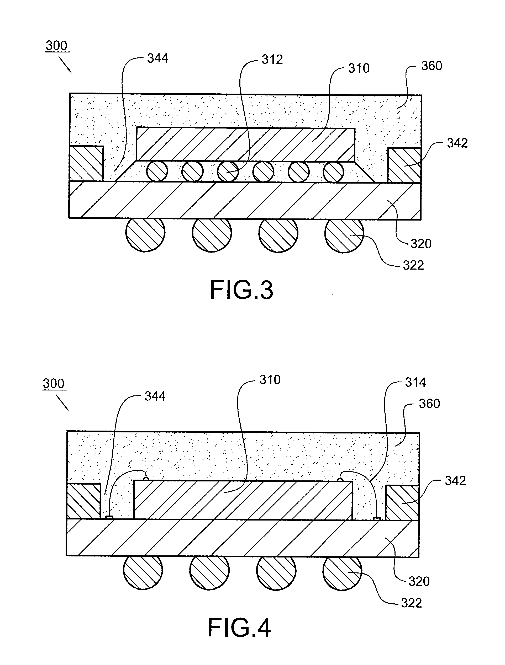
[0024]Referring to FIG. 3, it depicts a semiconductor package 100 according to an embodiment of the present invention. The semiconductor package 300 includes a carrier (e.g. thin type circuit board or substrate 320), a chip 310, a stiffener 342 and an encapsulant 360. The chip 310 is disposed on the substrate 320. The encapsulant is adapted to seal the chip 310 and cover the stiffener 342. A plurality of solder balls 322 are disposed on the substrate 320 for electrically connecting to an external circuit board (not shown) or an electronic device (not shown). In this embodiment, a plurality of bumps 312 are disposed between the chip 310 and the substrate 320 for electrically connecting the chip 310 to the substrate 320. Referring to FIG. 4, in another embodiment, a plurality of bonding wires 314 are adapted for electrically connecting the chip 310 to the substrate 320.

[0025]The stiffener 342 directly contacts the substrate 320, and is mounted on the substrate 320 by an attaching forc...


PUM


Abstract

A semiconductor package includes a carrier, a chip, a stiffener and an encapsulant. The chip is disposed on the carrier. The stiffener is disposed around the chip, directly contacts the carrier, and is mounted on the carrier. The encapsulant is adapted to seal the chip and the stiffener.

Description

CROSS REFERENCE TO RELATED APPLICATION[0001]This application claims the priority benefit of Taiwan Patent Application Serial Number 097119025, filed on May 23, 2008, the full disclosure of which is incorporated herein by reference.BACKGROUND OF THE INVENTION[0002]1. Field of the Invention[0003]The present invention generally relates to a package, and more particularly to a semiconductor package, wherein the mechanical robustness of a stiffener that can prevent a carrier (e.g. substrate) from warping during subsequent thermal processes. Also, the stiffener can be directly mounted on the carrier by the attaching force of an encapsulant. It is not necessary that the stiffener is attached on the carrier by an extra adhesive, thereby decreasing the processing step of the semiconductor package.[0004]2. Description of the Related Art[0005]Due to chips having high performance are required, a chip package having a thin type substrate is increasingly put in use. For example, the chip package ...

Claims


Application Information

Patent Timeline
Patent Type & Authority Patents(United States)
IPC IPC(8): H01L23/02H01L21/44
CPCH01L21/561H01L23/16H01L23/3128H01L24/97H01L2224/16H01L2224/48091H01L2224/97H01L2924/01027H01L2924/14H01L2924/1433H01L2924/15311H01L2924/00014H01L2224/81H01L24/48H01L2924/181H01L2224/16227H01L2224/32225H01L2224/48227H01L2224/73204H01L2224/73265H01L2924/3511H01L2924/00012H01L2224/45099H01L2224/45015H01L2924/207H01L2224/83H01L2924/00H01L2224/16225
Inventor HU, CHIA CHIENLIU, CHAO CHENGLIU, CHIENCHUNG, CHIH MING
Owner ADVANCED SEMICON ENG INC
Why Eureka
Try Eureka