

High density test structure array to support addressable high accuracy 4-terminal measurements
a test structure and high-density technology, applied in the field of device under test arrays, can solve the problems of increasing the severity of soft failure events, systematic faults, and failures of electricly measurable faults, and achieve the effect of reducing the amount of logic necessary and reducing the necessary area
- Summary
- Abstract
- Description
- Claims
- Application Information
AI Technical Summary
Benefits of technology
Problems solved by technology
Method used
Image

Examples
Embodiment Construction
[0033]An invention is described for circuitry that enables testing of devices under test (DUTs), which are designed and fabricated on a semiconductor wafer, and then fabricated into test chips. The DUTs can take many forms, and the type of DUT used will depend on the type of testing being performed. In some examples, a chip may include multiple types of DUTs, so that different characteristics can be tested from a single chip.
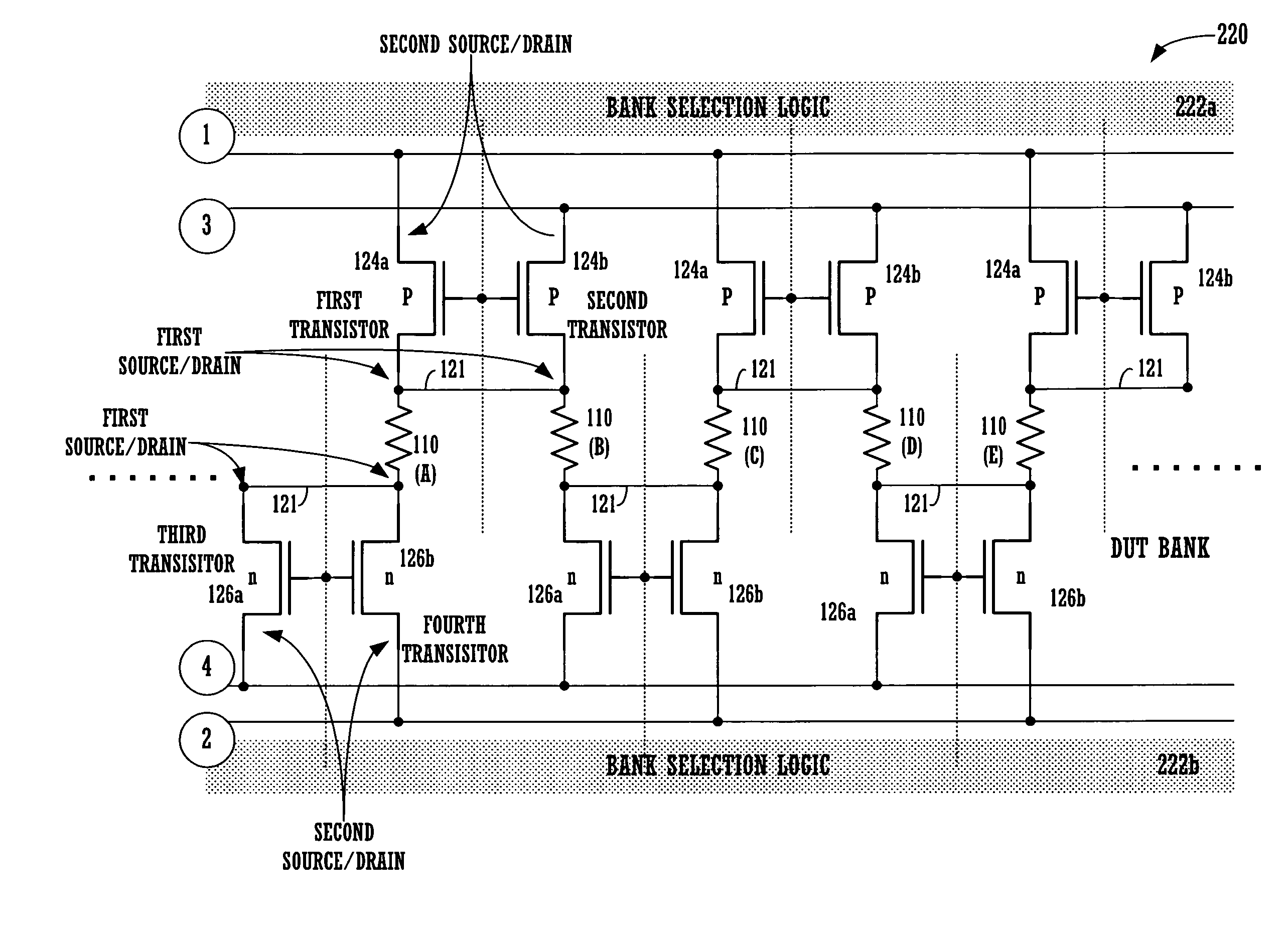
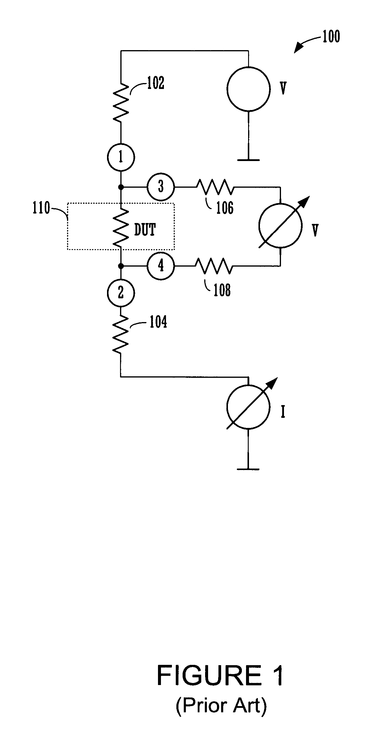
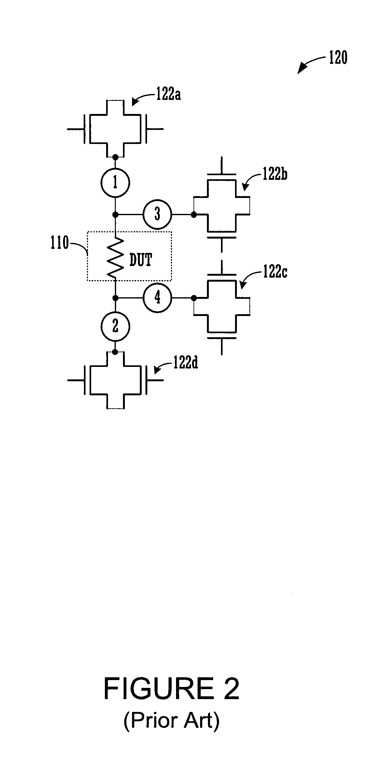
[0034]The testing of the DUTs, in accordance with the disclosed embodiments, is related to accurate four (4) terminal measurement point (TMP) testing. As noted above, 4-TMP testing is known, however, current 4-TMP testing circuitry is large, takes up too much space, and is not well suited to carry out localization during soft fail testing, nor efficient hard fail testing. In accordance with one embodiment, the 4-TMP testing circuitry utilizes single transistors to provide access to each of terminal measurement point (i.e., (1), (2), (3) and (4)). In another embo...
PUM
 Abstract
Description
Claims
Application Information