Thin film transistor substrate and method of manufacturing the same

a thin film transistor and substrate technology, applied in non-linear optics, instruments, optics, etc., can solve the problems of wavy noise, high manufacturing cost of thin film transistors, and occurrence of wavy noise, so as to prevent overetching and reduce manufacturing costs and time.

Active Publication Date: 2011-03-08
LG DISPLAY CO LTD
View PDF6 Cites 5 Cited by
  • Summary
  • Abstract
  • Description
  • Claims
  • Application Information

AI Technical Summary

Benefits of technology

[0011]An object of embodiments of the invention is to reduce a manufacturing cost and time of a flat panel display device having a thin film transistor.
[0012]Another object of embodiments of the invention is to prevent an over-etching during manufacturing of a thin film transistor in a flat panel display device.
[0014]Another object of embodiments of the invention is to reduce a wavy noise and improve the visual quality of a flat panel display device.

Problems solved by technology

However, the manufacturing cost of the thin film transistor is high due to the use of a 5-photomask process.
This results in the occurrence of a wavy noise.
The wavy noise is caused by interference generated between the active layer and the pixel electrode when leakage current in the active layer occurs due to light form a backlight unit.
The wavy noise generates moiré fringe on an image displayed on the liquid crystal panel, thereby reducing the display quality of the liquid crystal display.
However, a separate photomask process for forming the etch stopper is added such that there is again the problem of a complicated five photomask process, which increases manufacturing cost of the thin film transistor substrate.

Method used


Image

  • Thin film transistor substrate and method of manufacturing the same
  • Thin film transistor substrate and method of manufacturing the same
  • Thin film transistor substrate and method of manufacturing the same

Examples


Embodiment Construction

[0024]Reference will now be made in detail to exemplary embodiments of the invention, which are illustrated in the accompanying drawings.

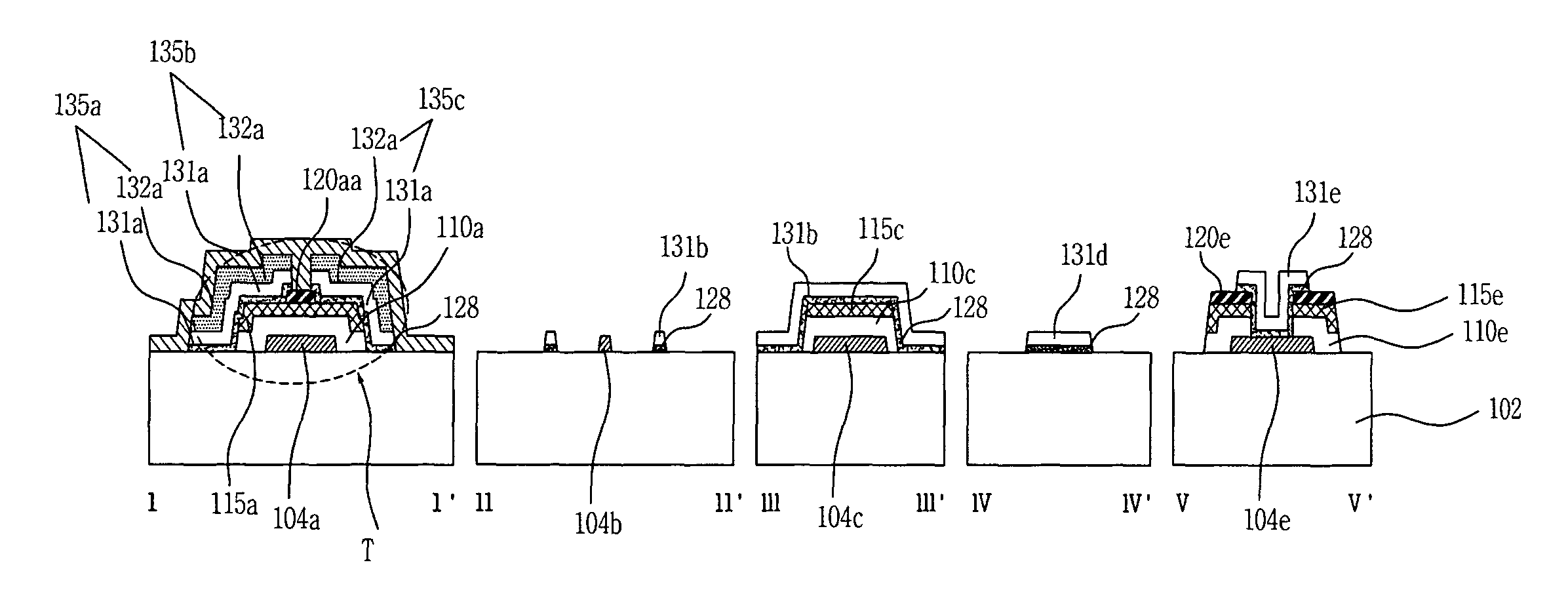
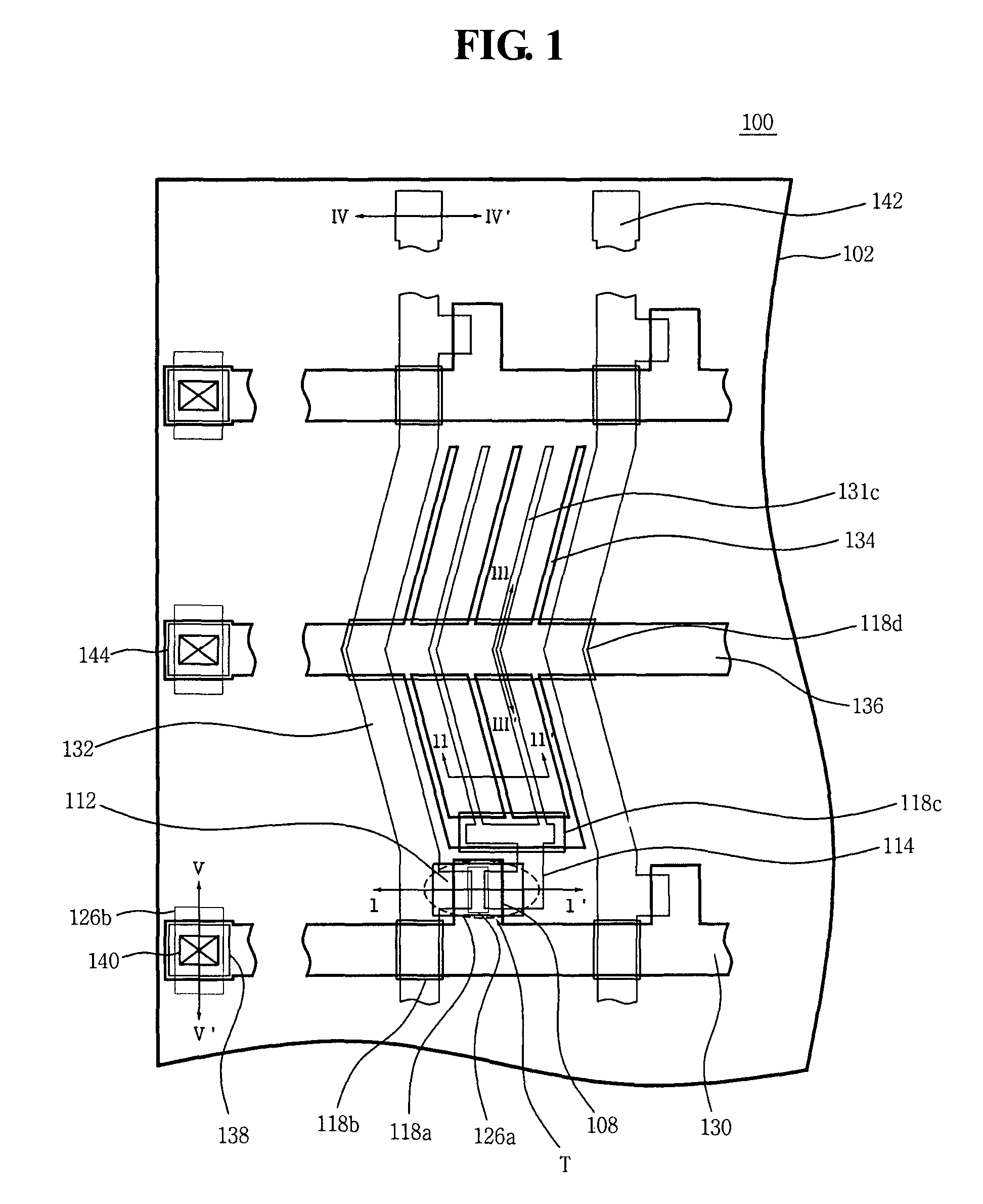
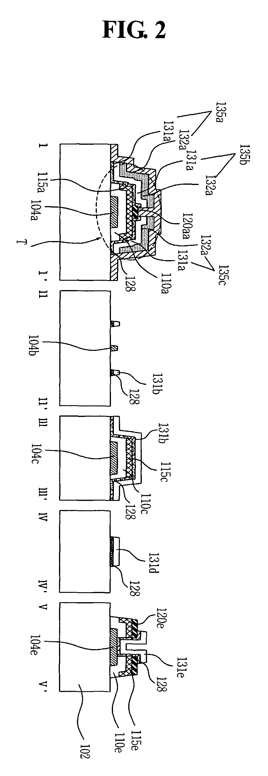
[0025]FIG. 1 is a plane view of a thin film transistor substrate according to a first embodiment. FIG. 2 is a cross-sectional view taken along lines I-I′, II-II′, III-III′, IV-IV′, and V-V′ of FIG. 1. Referring to FIGS. 1 and 2, a flat panel display, such as a liquid crystal display or an organic light emitting device, can include a thin film transistor substrate 100 according to the first embodiment. For instance, in the case where the liquid crystal display includes the thin film transistor substrate 100, the thin film transistor substrate 100 applies a driving voltage (for example, a data voltage and a common voltage) supplied from a driving circuit of the liquid crystal display to a liquid crystal layer of the liquid crystal display.

[0026]The thin film transistor substrate 100 includes a thin film transistor (T) with an etch stopper 120aa. The ...


PUM

PropertyMeasurementUnit
transparentaaaaaaaaaa
transparent conductiveaaaaaaaaaa
insulatingaaaaaaaaaa

Abstract

A method of fabricating a liquid crystal display device includes forming a gate electrode; forming a gate insulator on the gate electrode, an active layer on the gate insulator, and an etch stopper on the active layer; depositing an ohmic contact layer, a first metal layer and a second metal layer on the substrate; etching the ohmic contact layer, and the first and second metal layers to form ohmic contact patterns, and first and second metal patterns including source, drain and pixel electrodes using a single photomask.

Description

[0001]This application claims the benefit of Korean Patent Application No. 10-2006-0135467 filed on Dec. 27, 2006, which is hereby incorporated by reference.BACKGROUND[0002]1. Field of the Invention[0003]Embodiments of the present invention relate to a flat panel display, and more particularly, to a thin film transistor substrate for a flat panel display and a method of manufacturing the same.[0004]2. Description of the Related Art[0005]Flat panel displays such as liquid crystal displays (LCDs) and organic light emitting displays (OLEDs) include a thin film transistor substrate, on which a thin film transistor functioning as a switching device is formed, for active matrix driving. The liquid crystal display generally displays an image using electrooptic characteristics of liquid crystal molecules in a liquid crystal layer.[0006]The liquid crystal display includes a color filter substrate and a thin film transistor substrate which face each other with the liquid crystal layer sandwic...

Claims


Application Information

Patent Timeline
Patent Type & Authority Patents(United States)
IPC IPC(8): G02F1/1368
CPCG02F1/1368G02F1/134363G02F2001/13625G02F1/13625G02F1/136
Inventor YANG, JOON YOUNG
Owner LG DISPLAY CO LTD
Why Eureka
Try Eureka