Universal solder pad

a solder pad and universal technology, applied in the field of solder pads, can solve the problems of deterioration of electrical properties of integrated circuits, and tombstone defects, and achieve the effect of improving cost effectiveness

Inactive Publication Date: 2011-03-29
DELTA ELECTRONICS INC
View PDF4 Cites 10 Cited by
  • Summary
  • Abstract
  • Description
  • Claims
  • Application Information

AI Technical Summary

Benefits of technology

[0010]It is an object of the present invention to provide a universal solder pad for use with different-sized SMD components so as to enhance cost effectiveness.
[0011]Another object of the present invention provide a universal solder pad for minimizing the undesired effects such as oblique alignment, deviation and / or tombstone defects.
[0012]In accordance with an aspect of the present invention, there is provided a universal solder pad of a circuit carrier for use with a plurality of SMD components having different sizes. Each of the SMD components includes a first conductive part and a second conductive part. The universal solder pad includes a first pad unit and a second pad unit. The first pad unit is electrically connected to the first conductive part of the SMD component. The second pad unit is electrically connected to the second conductive part of the SMD component. Each of the first pad unit and the second pad unit includes a main portion and a first extension portion. The first extension portion is extended from a first sidewall of the main portion and includes a first border, a second border and a third border. The second border and the third border of the first extension portion are parallel with each other for facilitating alignment of the first and second conductive parts of the SMD component with respect to the first pad unit and the second pad unit.
[0013]In accordance with another aspect of the present invention, there is provided a solder pad of a circuit carrier for use with a SMD component. The SMD component includes a first conductive part and a second conductive part. Each of the first pad unit and the second pad unit includes a main portion and a first extension portion. The first extension portion is extended from a first sidewall of the main portion and includes a first border, a second border and a third border. The second border and the third border of the first extension portion are parallel with each other for facilitating alignment of the first and second conductive parts of the SMD component with respect to the first pad unit and the second pad unit.

Problems solved by technology

Due to the very small size and spacing of the SMD components, there are also some drawbacks.
In addition, a solder paste, which exhibits excessive out-gassing during the initial stages of the melting of the solder powder, will also result in tombstone defects.
In a case that the SMD components fail to be well bonded on the corresponding solder pads, the electrical properties of the integrated circuit are deteriorated.
Under this circumstance, the electrical properties of the integrated circuit will be deteriorated and the circuit board 11 is not aesthetically pleasing.
Therefore, a tombstone defect is resulted and the SMD component 10 is no longer electrically connected to the circuit board 11.
Therefore, the solder pads are not cost-effective.

Method used


Image

  • Universal solder pad
  • Universal solder pad
  • Universal solder pad

Examples


first embodiment

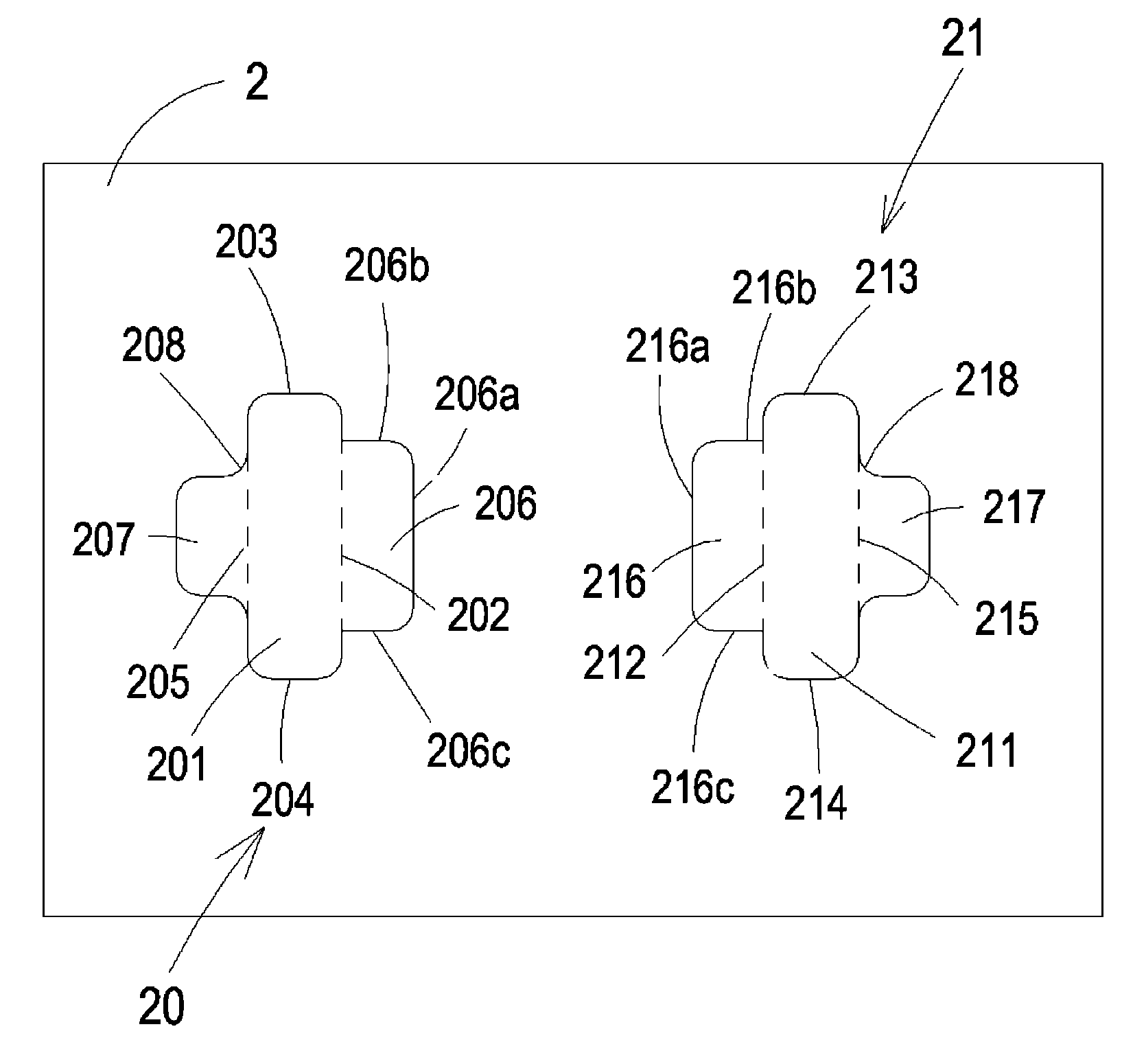
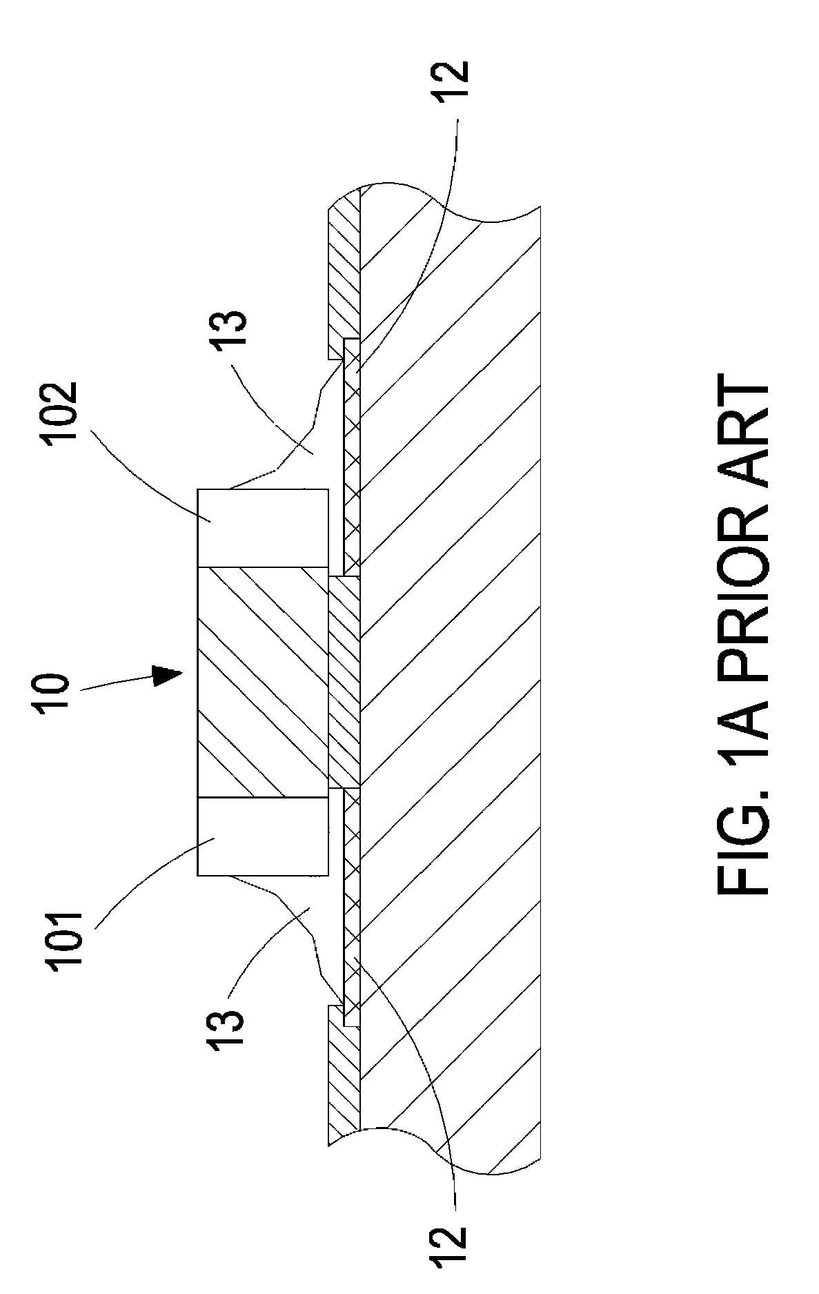
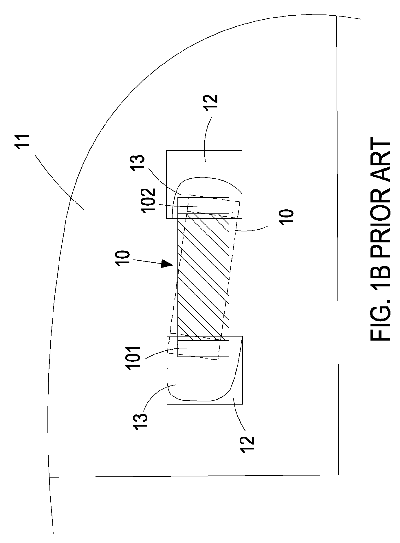
[0035]Please refer to FIG. 5A, which is a schematic cross-sectional view illustrating the first SMD component mounted on the universal solder pad according to the present invention. As shown in FIG. 5A, the first conductive part 271 and the second conductive part 272 of the first SMD component 27 are attached on the first pad unit 20 and the second pad unit 21 via the solder paste 26. Since the width of the conductive part 271 (272) is smaller than the first border 206a (216a) of the first extension portion 206 (216) and the second border 206b (216b) is parallel with the third border 206c (216c), the second borders 206b 216b and the third borders 206c, 216c may function as retaining marks for facilitating alignment of the first conductive part 271 and the second conductive part 272 of the first SMD component 27 with respect to the first pad unit 20 and the second pad unit 21. As a consequence, the possibility of causing the oblique alignment is reduced. In addition, the second borde...

second embodiment

[0040]Please refer to FIG. 8A, which is a schematic cross-sectional view illustrating the first SMD component mounted on the universal solder pad according to the present invention. As shown in FIG. 8A, the first conductive part 271 and the second conductive part 272 of the first SMD component 27 are attached on the first pad unit 20 and the second pad unit 21 via the solder paste 26. Since the width of the conductive part 271 (272) is smaller than the first border 206a (216a) of the first extension portion 206 (216) and the second border 206b (216b) is parallel with the third border 206c (216c), the second borders 206b 216b and the third borders 206c, 216c may function as retaining marks for facilitating alignment of the first conductive part 271 and the second conductive part 272 of the first SMD component 27 with respect to the first pad unit 20 and the second pad unit 21. As a consequence, the possibility of causing the oblique alignment is reduced. In addition, the second borde...


PUM


Abstract

A universal solder pad is used with a plurality of SMD components having different sizes. Each SMD component includes a first conductive part and a second conductive part. The universal solder pad includes a first pad unit and a second pad unit. The first and second pad units are electrically connected to the first and second conductive parts of the SMD component, respectively. Each of the first and second pad units includes a main portion and a first extension portion. The first extension portion is extended from a first sidewall of the main portion and includes a first border, a second border and a third border. The second border and the third border of the first extension portion are parallel with each other for facilitating alignment of the first and second conductive parts of the SMD component with respect to the first pad unit and the second pad unit.

Description

FIELD OF THE INVENTION[0001]The present invention relates to a solder pad, and more particularly to a universal solder pad for use with different-sized SMD components.BACKGROUND OF THE INVENTION[0002]Conventionally, a pin-through-hole technology (PTHT) is employed to mount electronic components onto one side of a printed circuit board through pin-through-hole connections. Since a plurality of through holes corresponding to the pins of the electronic components are drilled in the printed circuit board and the solder joints between the electronic components and the electronic components are very large, the pin-through-hole technology may be applied to the relatively low-density integrated circuits.[0003]With increasing progress of fabricating integrated circuits, the semiconductor packages are developed toward minimization and high integration. As a consequence, the requirement of increasing the pin density of the semiconductor packages becomes more important. Recently, a surface moun...

Claims


Application Information

Patent Timeline
Patent Type & Authority Patents(United States)
IPC IPC(8): H05K7/10
CPCH05K1/111H05K3/3442H05K3/3452H05K1/0295H05K2201/09381H05K2201/099H05K2201/09954H05K2201/10636H05K2203/058Y02P70/50
Inventor HUANG, CHUN-LINE
Owner DELTA ELECTRONICS INC
Why Eureka
Try Eureka