
Reflective semiconductor optical amplifier (R-SOA) with dual buried heterostructure

a semiconductor optical amplifier and heterostructure technology, applied in semiconductor lasers, optical elements, instruments, etc., can solve the problems of reducing the reflectivity of the emission surface, difficult to form an ar coating of only 0.1% or less on the emission surface, and inconvenient use of sld as a light source, etc., to achieve low current, low threshold current, and consuming a small amount of power

Inactive Publication Date: 2011-04-05
ELECTRONICS & TELECOMM RES INST
View PDF11 Cites 10 Cited by
  • Summary
  • Abstract
  • Description
  • Claims
  • Application Information

AI Technical Summary

Problems solved by technology

However, in general, it is very difficult to form an AR coating of only 0.1% or less on an emission surface of a FP-LD in order to prevent oscillation.
In this case, the reflectivity of the emission surface can be reduced, but the SLD is not suitable as a light source used for a WDM-PON due to a high threshold current and operating current.
However, such an R-SOA requires a light source consuming a small amount of power at low threshold and operating currents to be used in a WDM-PON.

Method used


Image

  • Reflective semiconductor optical amplifier (R-SOA) with dual buried heterostructure
  • Reflective semiconductor optical amplifier (R-SOA) with dual buried heterostructure
  • Reflective semiconductor optical amplifier (R-SOA) with dual buried heterostructure

Examples


Embodiment Construction

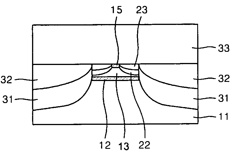
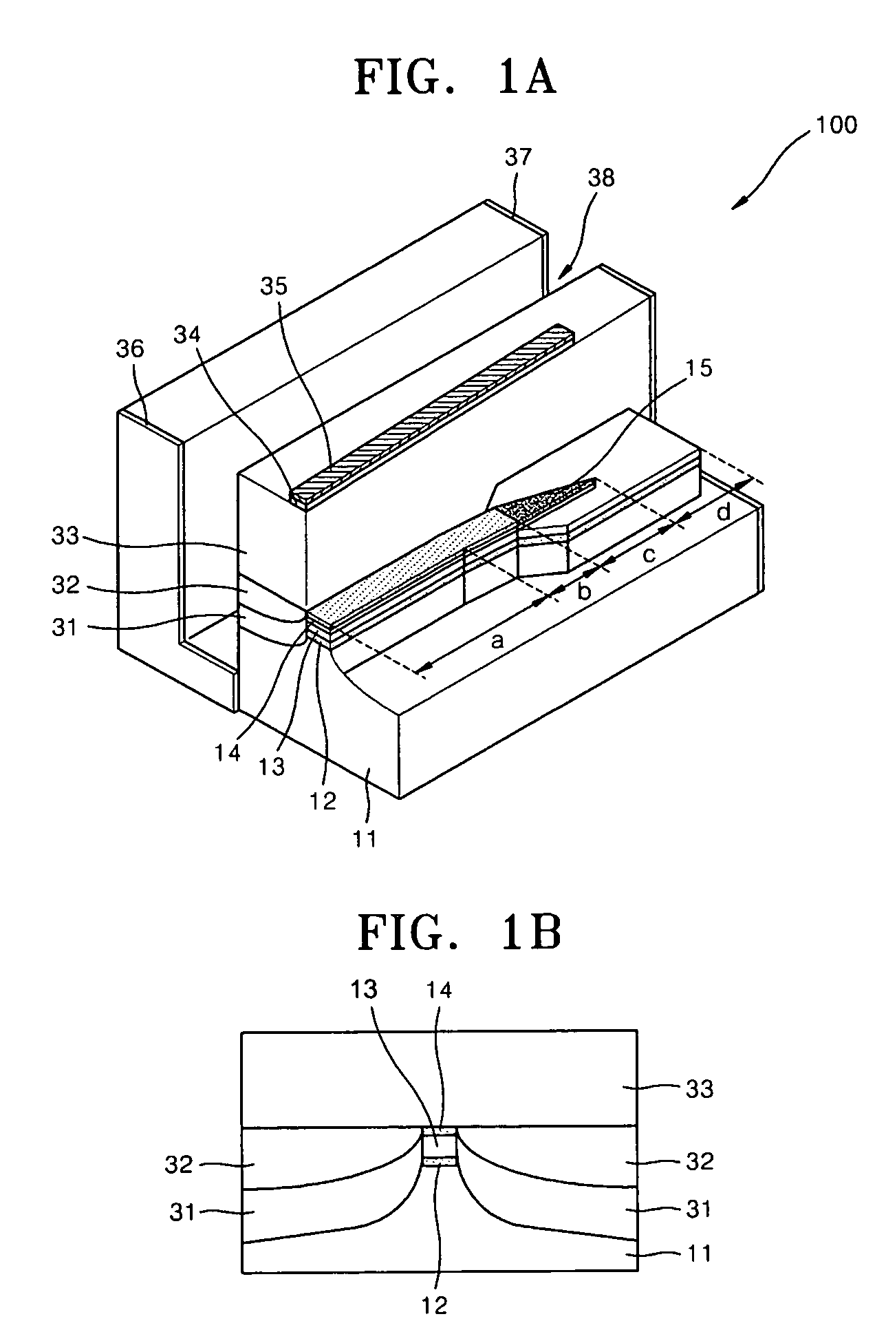
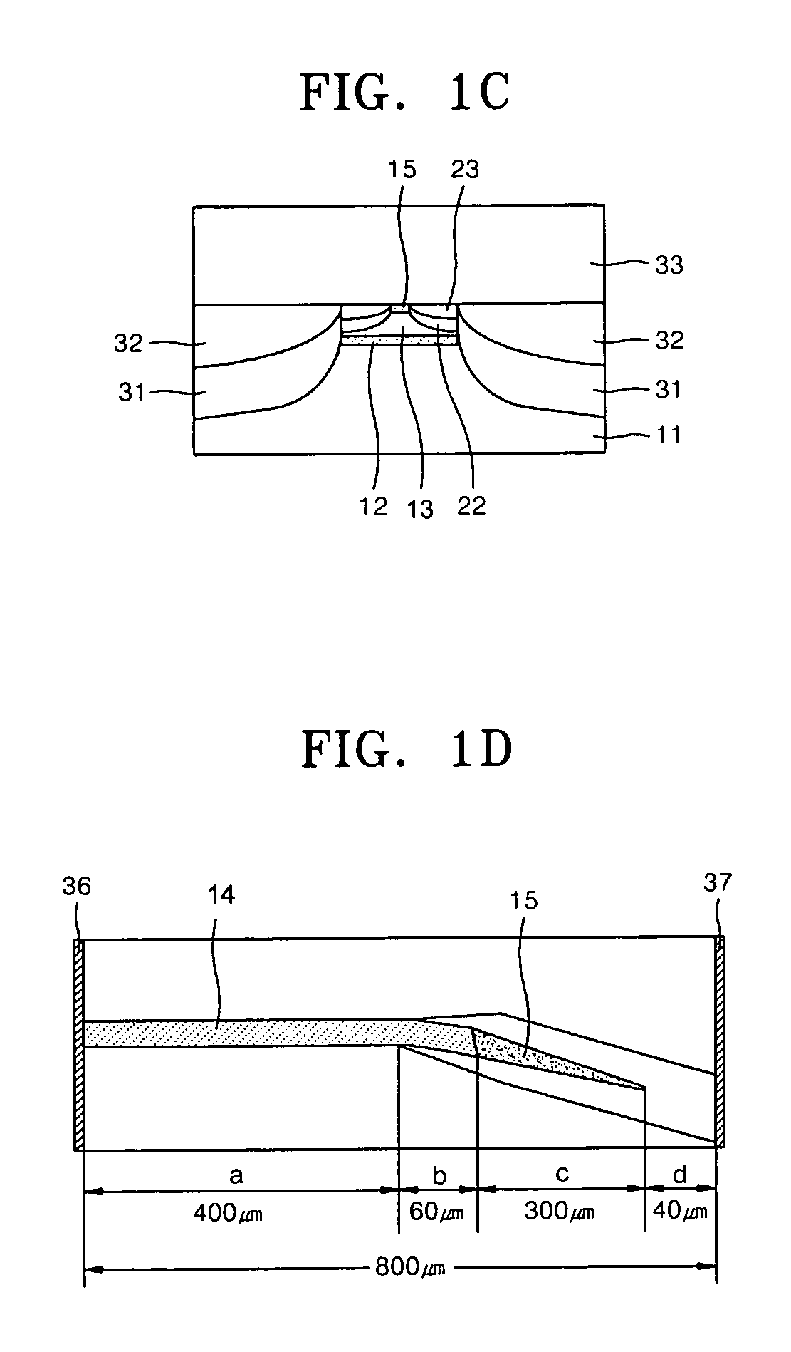
[0023]The present invention will now be described more fully with reference to the accompanying drawings, in which exemplary embodiments of the invention are shown. The invention may, however, be embodied in many different forms and should not be construed as being limited to the embodiments set forth herein; rather, these embodiments are provided so that this disclosure will be thorough and complete, and will fully convey the concept of the invention to those skilled in the art. In the drawings, the thicknesses of layers and regions are exaggerated for clarity. Like reference numerals in the drawings denote like elements, and thus their description will be omitted.

[0024]In embodiments of the present invention, active layers of a superluminescent diode (SLD) and a reflective semiconductor optical amplifier (R-SOA) used in an optical line terminal (OLT) and an optical network unit (ONU) of a Wavelength Division Multiplexing Passive Optical Network (WDM-PON) have the same structure. H...


PUM


Abstract

Provided are a reflective semiconductor optical amplifier (R-SOA) and a superluminescent diode (SLD). The R-SOA includes: a substrate; an optical waveguide including a lower clad layer, an active layer independent of the polarization of light, and an upper clad layer sequentially stacked on the substrate, the optical waveguide comprising linear, curved, and tapered waveguide areas; and a current blocking layer formed around the optical waveguide to block a flow of current out of the active layer, wherein the linear and curved waveguide areas have a single buried hetero (BH) structure, and the tapered waveguide area has a dual BH structure.

Description

CROSS-REFERENCE TO RELATED PATENT APPLICATION[0001]This application claims the benefit of Korean Patent Application No. 10-2006-0124135, filed on Dec. 7, 2006, in the Korean Intellectual Property Office, the disclosure of which is incorporated herein in its entirety by reference.BACKGROUND OF THE INVENTION[0002]1. Field of the Invention[0003]This work was supported by the IT R&D program of MIC / IITA.[2005-S-051-02, Photonic device integrated module for optical access network][0004]The present invention relates to a semiconductor optical amplifier (SOA), and more particularly, to a reflective SOA (R-SOA) and a superluminescent diode (SLD) having low operating and threshold currents.[0005]2. Description of the Related Art[0006]An optical line terminal (OLT) and an optical network unit (ONU) used in a Wavelength Division Multiplexing Passive Optical Network (WDM-PON) have several types of light sources. According to a recently announced paper in IEEE PTL, vol. 18, no. 13, pp. 1436-1438,...

Claims


Application Information

Patent Timeline
Patent Type & Authority Patents(United States)
IPC IPC(8): H01S5/00H01L29/06H01L33/20H01L33/00
CPCG02B6/1228H01L33/0045H01S5/026H01S5/50H01S5/227H01S5/028G02B2006/121H01S5/101H01S5/1014H01S3/0941
Inventor OH, SU HWANPARK, SAHNGGIBAEK, YONGSOONOH, KWANG-RYONG
Owner ELECTRONICS & TELECOMM RES INST
Learn More