Superluminescent diode including active layer formed of various sized quantum dots and method of manufacturing the same

a technology of superluminescent diodes and active layers, which is applied in the direction of diodes, semiconductor devices, electrical apparatus, etc., can solve the problems of high optical power that cannot be generated with currents above a certain extent, the coating process capable of ensuring the reflection rate of 10sup>5/sup>needs very precise and strict work, and reproducibility, mass production and price competitiveness cannot be anticipated, etc., to achieve the effect of high optical power

Inactive Publication Date: 2006-04-27
KOREA INST OF SCI & TECH
View PDF2 Cites 11 Cited by
  • Summary
  • Abstract
  • Description
  • Claims
  • Application Information

AI Technical Summary

Benefits of technology

[0013] The present invention provides a superluminescent diode with wide wavelength bandwidth and high optical power, as well as a method of manufacturing the same.

Problems solved by technology

Accordingly, there is a problem in that high optical power cannot be generated with currents above a certain extent due to the thermal energy accumulated in the LED.
However, the AR coating process capable of guaranteeing the reflection rate of 10−5 needs very precise and strict work.
Thus, reproducibility, mass production and price competitiveness cannot be anticipated in the manufacturing process of superluminescent diode having the electrode perpendicular to the mirrored-sides of the active medium.
However, with conventional methods, it is difficult to get wide wavelength bandwidth and high optical power continuously.

Method used


Image

  • Superluminescent diode including active layer formed of various sized quantum dots and method of manufacturing the same
  • Superluminescent diode including active layer formed of various sized quantum dots and method of manufacturing the same
  • Superluminescent diode including active layer formed of various sized quantum dots and method of manufacturing the same

Examples


first embodiment

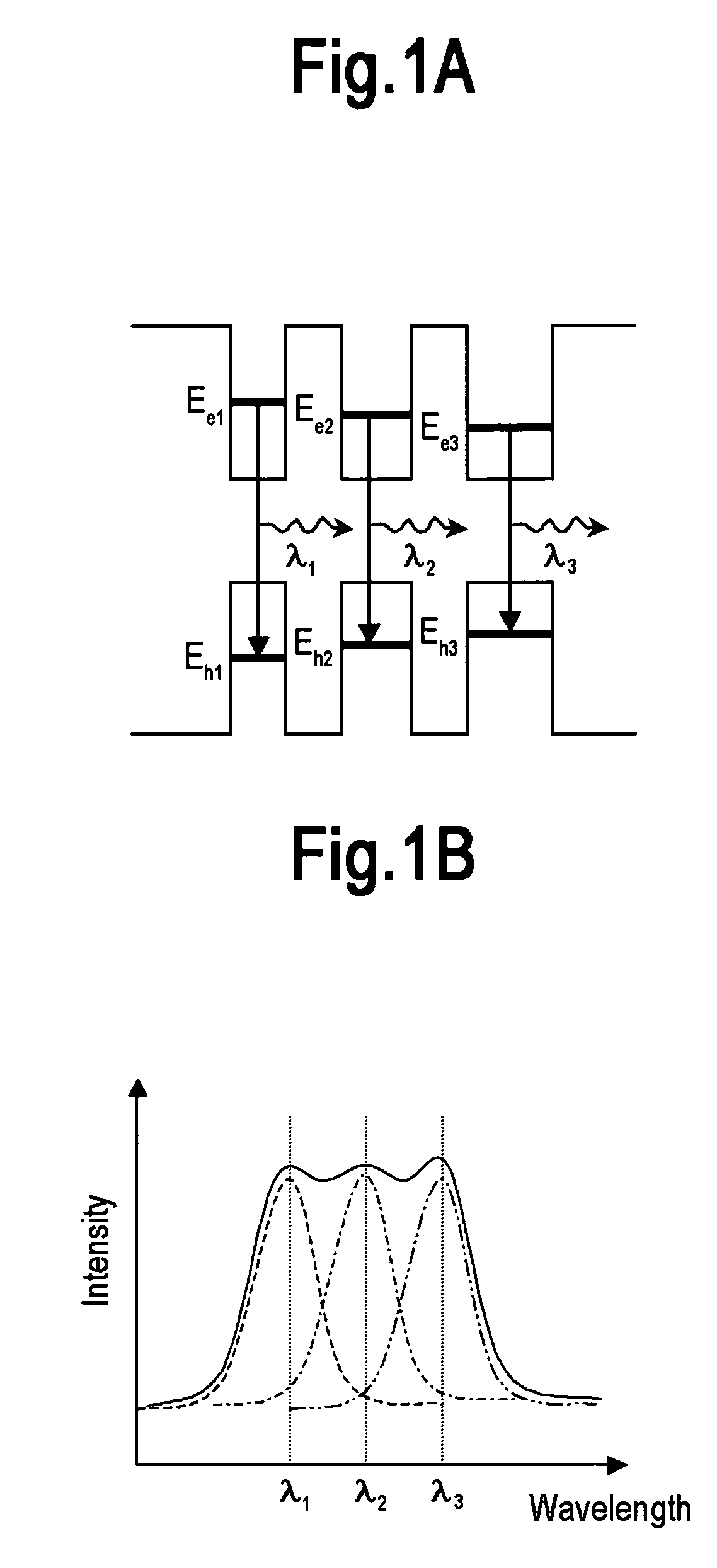
[0029]FIG. 4 is a schematic diagram showing an active layer formed of a multi-layer quantum dot structure, which has two different energy bands according to the present invention. The active layer has a chirped quantum dot (CQD) structure composed of three quantum dot layers and other three quantum dot layers emitting lights of 1.3 μm and 1.2 μm wavelength, respectively, when electrons and holes are recombined.

second embodiment

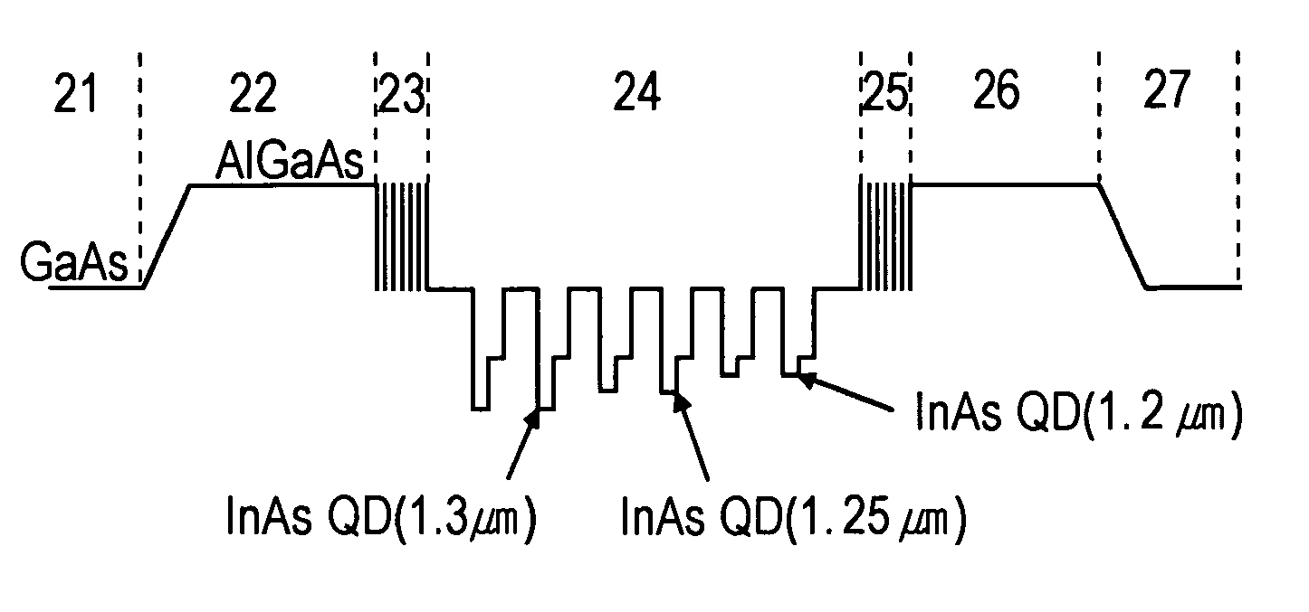
[0030]FIG. 5 is a schematic diagram showing an active layer formed with the CQD structure, which has at least three different energy bands in accordance with the present invention. The CQD structure includes two quantum dot layers, which emit light of 1.25 μm wavelength, between two quantum dot layers emitting lights of 1.3 μm wavelength and other two quantum layers emitting light of 1.2 μm wavelength. In FIG. 5, ‘21’ represents a GaAs substrate, ‘22’ and ‘26’ represent AlGaAs cladding layers, ‘23’ and ‘25’ represent superlattice layers, ‘24’ represents an active layer, and ‘27’ represents an ohmic layer. The active layer 24 has the same energy band as the conventional active layer formed with a chirped quantum well (CQW) structure, which includes a plurality of quantum wells having different thickness and composition. Therefore, lights having different wavelengths, 1.2 μm, 1.25 μm and 1.3 μm, which correspond to the energy level differences between the electrons and holes in the ac...


PUM


Abstract

The present invention provides a superluminescent diode, which has a wide wavelength bandwidth and a high optical power, and a method of manufacturing the same. The superluminescent diode includes an active layer having a chirped quantum dot (CQD) structure formed over the substrate, wherein the active layer emits lights of at least two different wavelengths.

Description

FIELD OF THE INVENTION [0001] The present invention generally relates to superluminescent diodes (SLD), and more particularly to a superluminescent diode including an active layer formed of various sized quantum dots and a method of manufacturing the same. BACKGROUND OF THE INVENTION [0002] A semiconductor light emitting device includes a p-n junction and emits energy in the form of light corresponding to an energy gap between an electron and a hole which are recombined when current is applied to the p-n junction. A light emitting diode (LED) and a laser diode are typical examples of the semiconductor light emitting device. [0003] The LED includes an active layer having a low energy-band gap, which is formed between semiconductor layers having high energy-band gaps. Light is spontaneously emitted from the active layer. The LED outputs light having wide bandwidth and low optical power of several mW. Generally, the optical power of the LED increases in proportion to the intensity of c...

Claims


Application Information

Patent Timeline
Patent Type & Authority Applications(United States)
IPC IPC(8): H01L33/00
CPCB82Y10/00H01L33/0045
Inventor HAN, IL KILEE, JUNG ILYOO, YOUNG CHAI
Owner KOREA INST OF SCI & TECH
Why Eureka
Try Eureka