
Optical wave plate with low wavelength sensitivity, large size and true zero order as well as preparation method and application of optical wave plate

A true zero-order, sensitive technology, applied in optics, optical components, lasers, etc., can solve the problems of few application occasions, small cutting angle range, and narrow wavelength bandwidth, and achieve wide application range, large cutting angle range, and wavelength The effect of bandwidth

Pending Publication Date: 2018-11-06
SHANDONG UNIV
View PDF15 Cites 2 Cited by
  • Summary
  • Abstract
  • Description
  • Claims
  • Application Information

AI Technical Summary

Problems solved by technology

The optional range of cutting angle is small, the wavelength bandwidth is narrow, the use range is narrow, and there are few applications

Method used


Image

  • Optical wave plate with low wavelength sensitivity, large size and true zero order as well as preparation method and application of optical wave plate
  • Optical wave plate with low wavelength sensitivity, large size and true zero order as well as preparation method and application of optical wave plate
  • Optical wave plate with low wavelength sensitivity, large size and true zero order as well as preparation method and application of optical wave plate

Examples


Embodiment 1

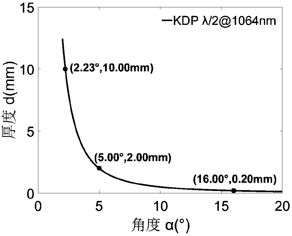
[0066] A large-size true zero-order optical wave plate with low wavelength sensitivity. The type of the wave plate is a half-wave plate; the material of the wave plate is KDP crystal; the aperture is 1cm, the thickness is 200μm, and the 1064nm true zero-order KDP half-wave Chip device, its cut angle α is 16.00°, such as figure 1 shown.

Embodiment 2

[0068] A large-size true zero-order optical wave plate with low wavelength sensitivity, the type of the wave plate is a half-wave plate; the material of the wave plate is KDP crystal; the diameter is 10cm, the thickness is 2mm, 1064nm true zero-order KDP half-wave Chip device, the cut angle α is 5.00°, such as figure 1 shown.

[0069] The experimental device for detecting the wavelength sensitivity of waveplates by polarization interferometry is as follows: Figure 9 shown. The polarizer and analyzer are parallel to each other, and the KDP or ADP half-wave plate is placed in the middle. The direction of the optical axis of the wave plate forms an included angle of 45° with the direction of transmission of the polarizer or analyzer. The light output intensity of the entire test system depends on the polarization state behind the wave plate. The change of wavelength affects the phase retardation of the wave plate, and then changes the polarization state of the output light a...

Embodiment 3

[0072] A large-size true zero-order optical wave plate with low wavelength sensitivity. The type of the wave plate is a half-wave plate; the material of the wave plate is KDP crystal; the aperture is 50cm, the thickness is 1cm, and the 1064nm true zero-order KDP half-wave Chip device, the cut angle α is 2.23°, such as figure 1 shown.


PUM


Abstract

The invention relates to an optical wave plate with low wavelength sensitivity, large size and true zero order as well as a preparation method and application of the optical wave plate. After the caliber and the thickness of the wave plate are determined, corresponding double refraction can be obtained according to the types of the wave plates and the central operating wavelength and further a space chamfer of a crystal is determined. The method has the greatest characteristics that the tangent direction of the crystal is flexibly selected according to the size of a device, and a traditional mode of processing a crystal wave plate along a fixed tangent direction is abandoned. Compared with a current widely-used crystal wave plate, the wave plate provided by the invention has the advantagesof convenience in processing, low cost, large size, high strength, low wavelength sensitivity and the like, is particularly suitable for phase retard and polarization conversion of large-caliber andwide-spectrum laser and is expected to realize important application in multiple optical and laser systems.

Description

technical field [0001] The invention relates to a large-size true zero-order optical wave plate with low wavelength sensitivity and a preparation method and application thereof, belonging to the technical field of polarization optics. Background technique [0002] Optical wave plate, also known as optical phase retarder, is an important optical component that uses birefringence to change the polarization state of light. It has a very wide range of applications in optical and laser devices related to light polarization, such as photoelasticity meters, polarimeters, and electro-optic Q-switched solid-state lasers. Generally speaking, wave plates can be divided into: true zero-order wave plates, multi-order wave plates, and composite zero-order wave plates composed of more than two wave plates. Compared with multi-order waveplates (phase delay>2π), zero-order waveplates (phase delay<2π), especially true zero-order waveplates, have low wavelength sensitivity (wide operati...

Claims


Application Information

Patent Timeline
Patent Type & Authority Applications(China)
IPC IPC(8): G02B5/30H01S3/10
CPCH01S3/10061G02B5/3083
Inventor 王正平孙洵任宏凯许心光
Owner SHANDONG UNIV
Learn More