

Semiconductor packaging method to save interposer
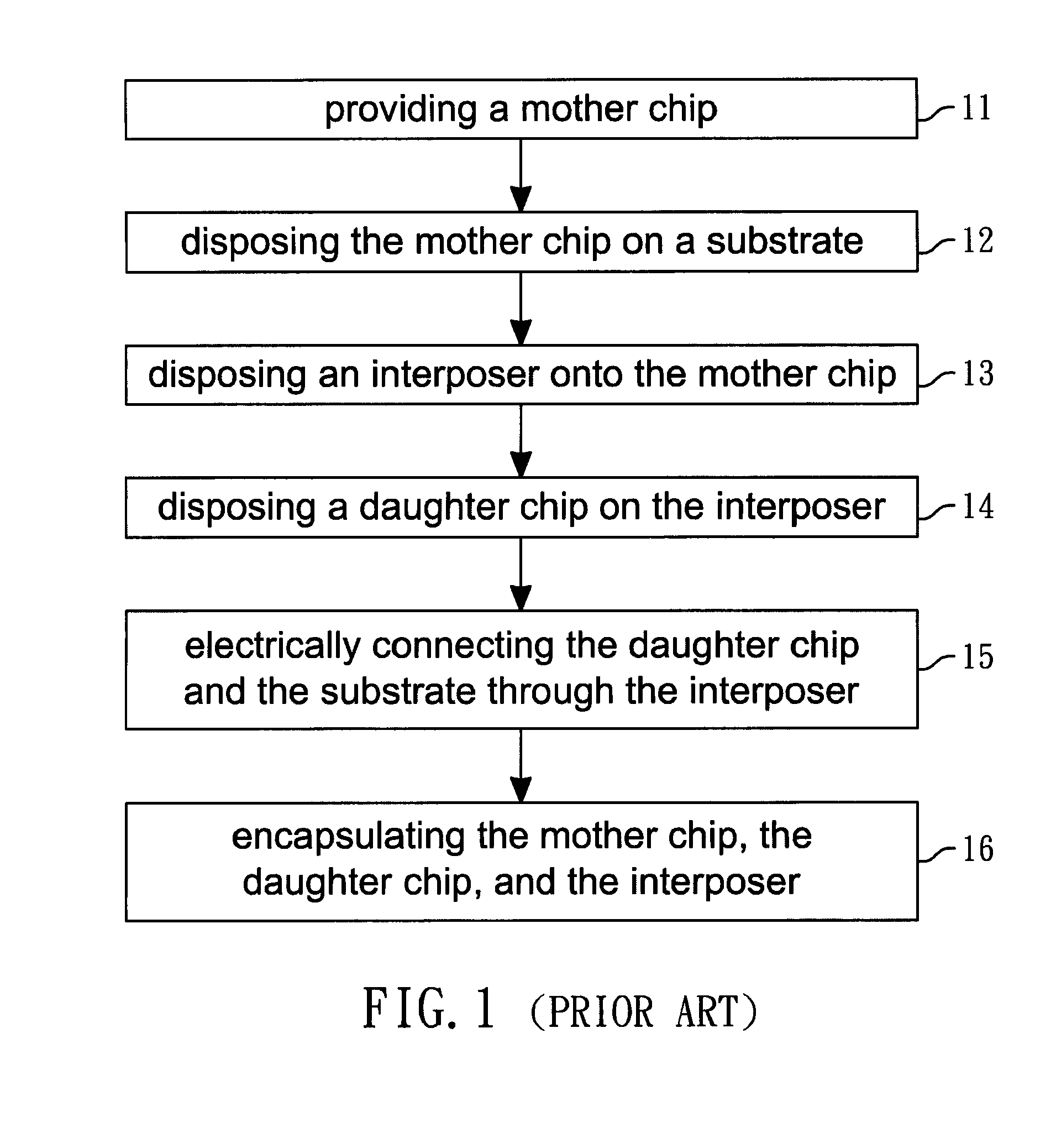
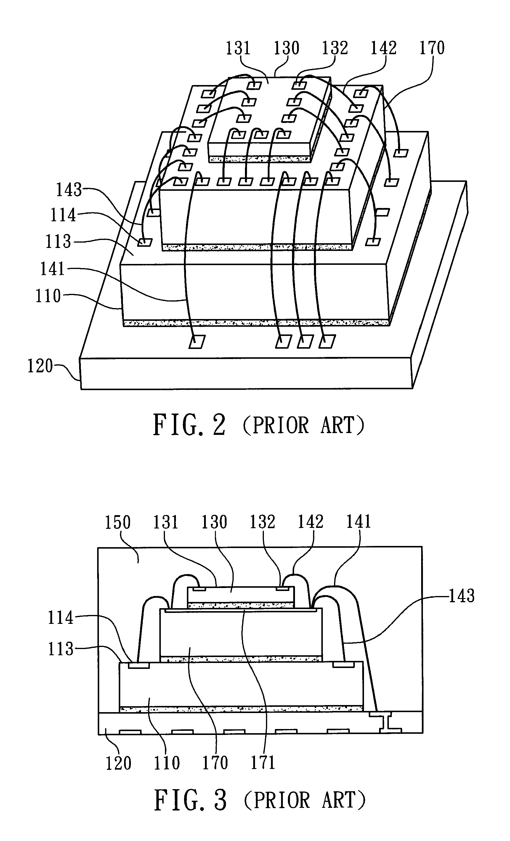
a technology of semiconductor devices and packaging methods, applied in the direction of semiconductor devices, semiconductor/solid-state device details, electrical apparatus, etc., can solve the problems of uncontrollable package warpage, increased overall package thickness, poor adhesion, etc., to prevent delamination and package warpage, reduce the overall package thickness
- Summary
- Abstract
- Description
- Claims
- Application Information
AI Technical Summary
Benefits of technology
Problems solved by technology
Method used
Image

Examples
Embodiment Construction
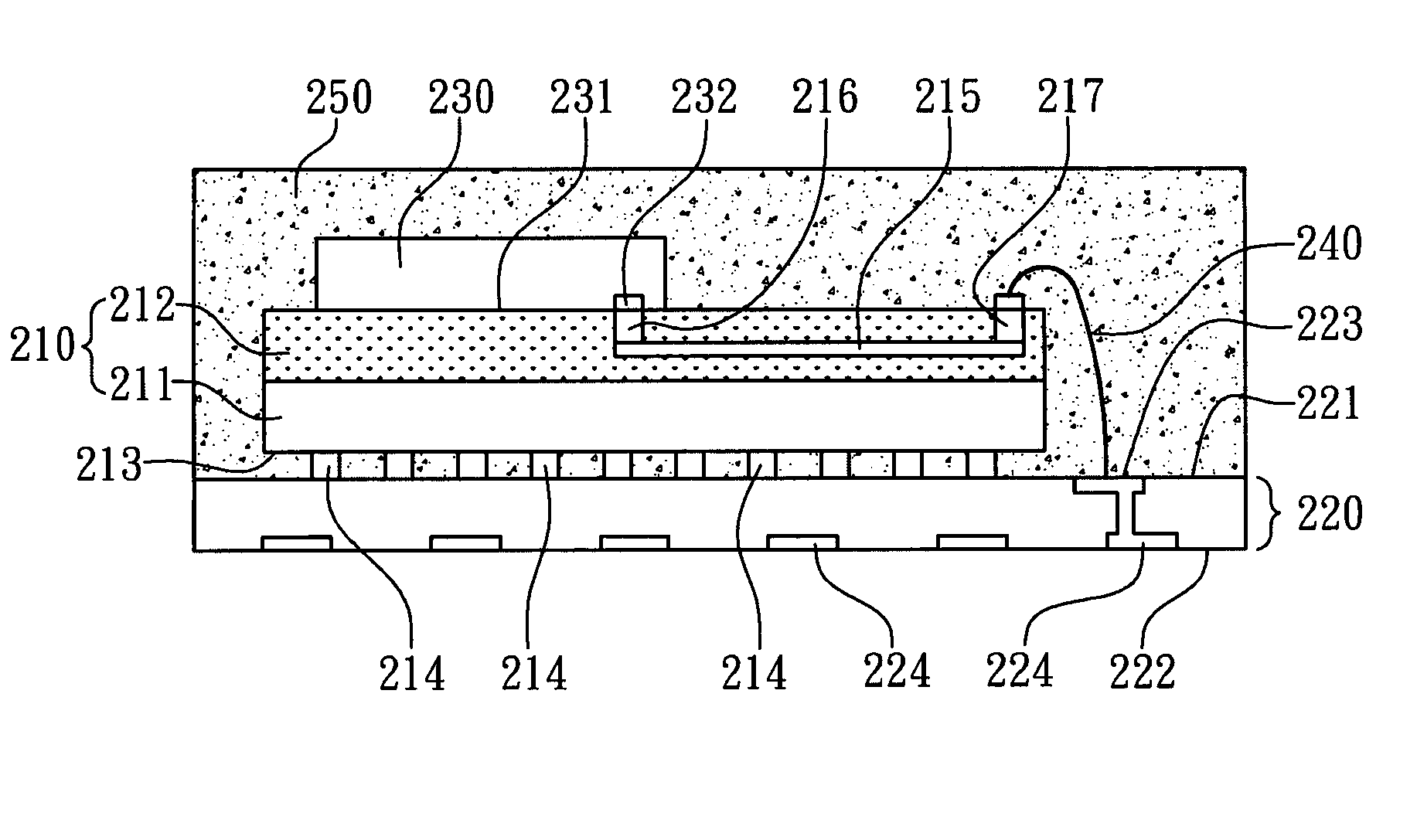
[0021]With reference to the attached drawings, the present invention is described by means of the embodiment(s) below where the attached drawings are simplified for illustration purposes only to illustrate the structures or methods of the present invention by describing the relationships between the components and assembly in the present invention. Therefore, the components shown in the figures are not expressed with the actual numbers, actual shapes, actual dimensions, nor with the actual ratio. Some of the dimensions or dimension ratios have been enlarged or simplified to provide a better illustration. The actual numbers, actual shapes, or actual dimension ratios can be selectively designed and disposed and the detail component layouts may be more complicated.
[0022]According to the preferred embodiment of the present invention, a semiconductor packaging method without an interposer is illustrated in FIG. 4 for a process flow block diagram, a semiconductor package fabricated accord...
PUM
 Abstract
Description
Claims
Application Information