Organic TFT, method of manufacturing the same and flat panel display device having the same

a flat panel display and organic technology, applied in the direction of transistors, solid-state devices, thermoelectric devices, etc., can solve the problems of channel layer, disconnection of wires in the channel region, and improper conductive conductivity, so as to avoid the pattern failure of an organic semiconductor layer

Inactive Publication Date: 2011-04-19
SAMSUNG DISPLAY CO LTD
View PDF63 Cites 6 Cited by
  • Summary
  • Abstract
  • Description
  • Claims
  • Application Information

AI Technical Summary

Benefits of technology

[0010]It is therefore an object of the present invention to provide an organic TFT in which a pattern failure of an organic semiconductor layer is avoided by reducing or eliminating a step difference between source and drain electrodes and a substrate.
[0012]It is further an object of the present invention to provide a flat panel display device having an organic TFT in which a step difference between source and drain electrodes and a substrate is reduced or eliminated.

Problems solved by technology

Therefore, if the organic semiconductor layer is too thick, the channel layer may not become properly conductive, or a high driving voltage must be applied to make the channel layer conductive.
When the organic semiconductor layer is thinner than the source and drain electrodes of metal wires, an edge portion of the source and drain electrodes can experience electrostatic discharge or can cause a pattern failure of a semiconductor layer due to poor step coverage, thus causing a disconnection of wires in the channel region.

Method used


Image

  • Organic TFT, method of manufacturing the same and flat panel display device having the same
  • Organic TFT, method of manufacturing the same and flat panel display device having the same
  • Organic TFT, method of manufacturing the same and flat panel display device having the same

Examples


Embodiment Construction

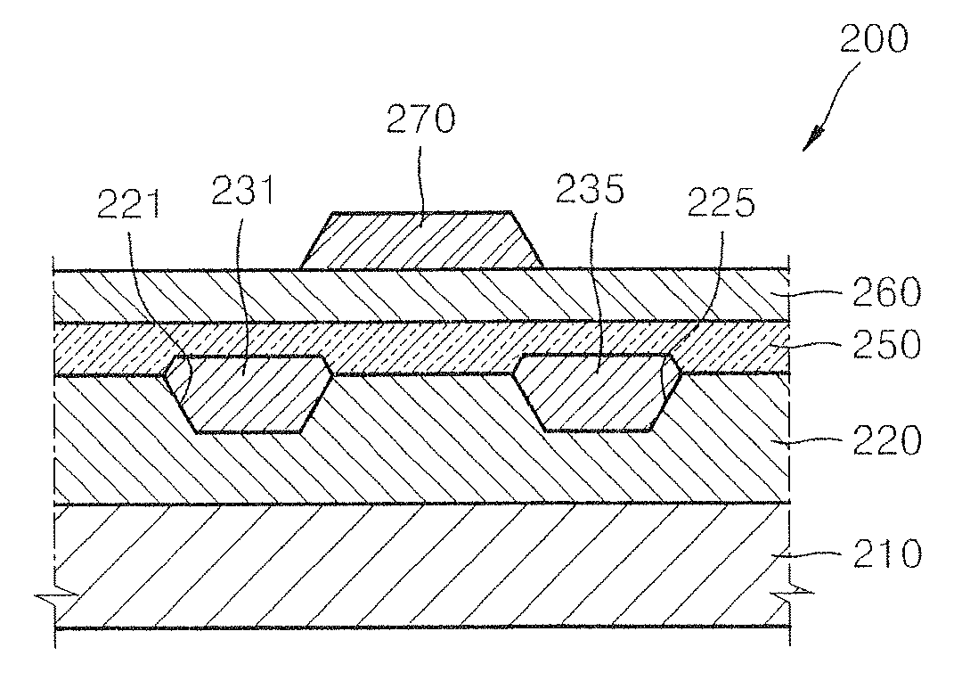
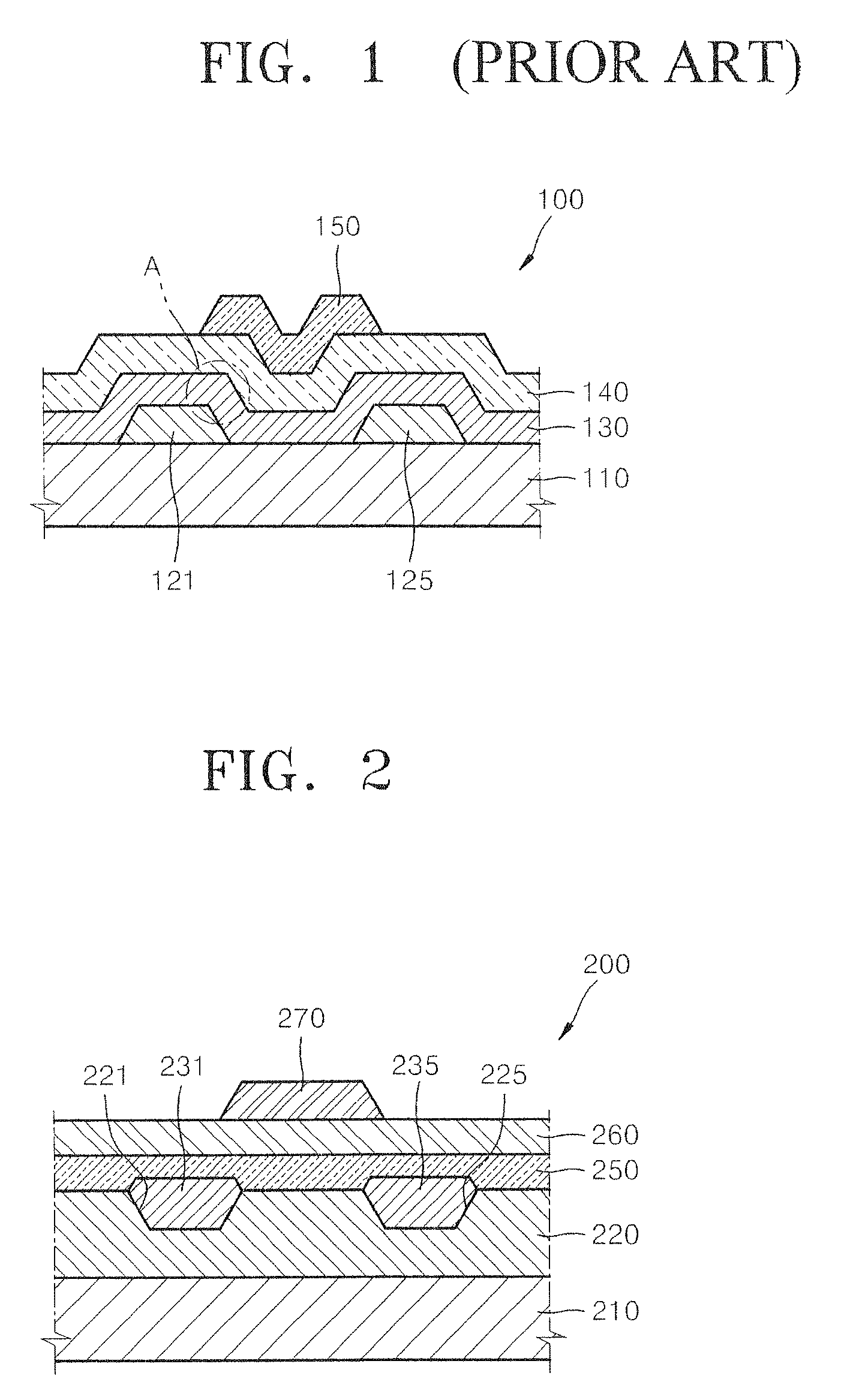
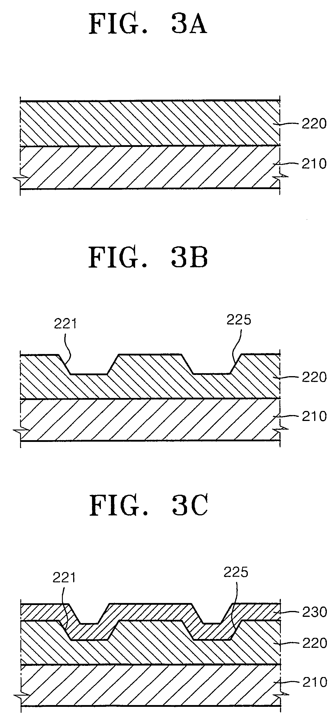
[0025]Turning now to the figures, FIG. 1 is a cross-sectional view of a top gate type organic TFT 100. Referring to FIG. 1, the organic TFT 100 includes source and drain electrodes 121 and 125 formed on a substrate 110, an organic semiconductor layer 130 formed on the source and drain electrodes 121 and 125, a gate insulating film 140 formed on the organic semiconductor layer 130, and a gate electrode 150 formed on the gate insulating film 140.

[0026]After the source and drain electrodes 121 and 125 are formed on the substrate 110, the organic semiconductor layer 130 and the gate insulating film 140 are formed by coating or deposition. Specifically, when the organic semiconductor layer 130 is formed by coating, if the source and drain electrodes 121 and 125 are formed as thick metal wires, the organic semiconductor layer 130 must be coated to a thickness equal to or greater than the thickness of the metal wires. A portion of the organic semiconductor layer 130 between the source and ...


PUM


Abstract

An organic thin film transistor (TFT), a method of making and a display including the organic TFT. In the TFT, the disconnection of a channel region does not occur because a step difference between a substrate and source and drain electrodes is lessened or eliminated by forming the source and drain electrodes in grooves in a buffer film. The method of manufacturing the organic TFT includes forming a buffer film on a substrate, forming concave units separated by a distance from each other in the buffer film by etching the buffer film, forming an electrode layer on the buffer film, forming source and drain electrodes within the concave units by etching the electrode layer using a photolithography process, forming a semiconductor layer on the source and drain electrodes and on the buffer film, forming a gate insulating film on the semiconductor layer and forming a gate electrode on the gate insulating film.

Description

CLAIM OF PRIORITY[0001]This application makes reference to, incorporates the same herein, and claims all benefits accruing under 35 U.S.C. §119 from an application for OTFT AND FABRICATION METHOD THEREOF AND FLAT PANEL DISPLAY DEVICE WITH THE SAME earlier filed in the Korean Intellectual Property Office on 27 May 2005 and there duly assigned Serial No. 10-2005-0045189.BACKGROUND OF THE INVENTION[0002]1. Field of the Invention[0003]The present invention relates to a flat panel display device that includes an organic thin film transistor (TFT) in which a pattern failure of an organic semiconductor layer in the organic TFT can be avoided by preventing a step difference between the source and the drain electrodes and the substrate, a method of manufacturing the organic TFT, and a flat panel display device having the organic TFT.[0004]2. Description of the Related Art[0005]Organic TFTs are considered to be next generation driving devices, and many studies of organic TFTs are being conduc...

Claims


Application Information

Patent Timeline
Patent Type & Authority Patents(United States)
IPC IPC(8): H01L51/10
CPCH01L51/105H01L51/0541H01L51/0021H01L27/3274H10K59/125H10K71/60H10K10/464H10K10/84
Inventor LEE, HUN-JUNGSUH, MIN-CHULKOO, JAE-BON
Owner SAMSUNG DISPLAY CO LTD
Why Eureka
Try Eureka