Electro-optical device and electronic apparatus

a technology of optical devices and electronic devices, applied in non-linear optics, instruments, optics, etc., can solve the problems of affecting the quality of image display, and affecting the accuracy of image display, so as to suppress alignment failure and high-quality image display

Inactive Publication Date: 2010-07-29
SEIKO EPSON CORP
View PDF2 Cites 7 Cited by
  • Summary
  • Abstract
  • Description
  • Claims
  • Application Information

AI Technical Summary

Benefits of technology

[0007]An advantage of some aspects of the invention is that it provides an electro-optical device capable of achieving a high-quality ima...

Problems solved by technology

If a step difference is present in a surface of an underlying layer of the alignment film, smoothness of the shape of the surface of the alignment film is disturbed and alignment failure of the electro-optical material occurs.
In particular, in a liquid crystal device in which the pixel pitch is decreased under a requirement for high definition, it is difficult to uniformly form a concave-convex pattern over an entire image display region with high accuracy, from a technical point of view.
Then, the distribution of the electric field in the vicinities of the surfaces of the pixel electrodes are ...

Method used


Image

  • Electro-optical device and electronic apparatus
  • Electro-optical device and electronic apparatus
  • Electro-optical device and electronic apparatus

Examples


first embodiment

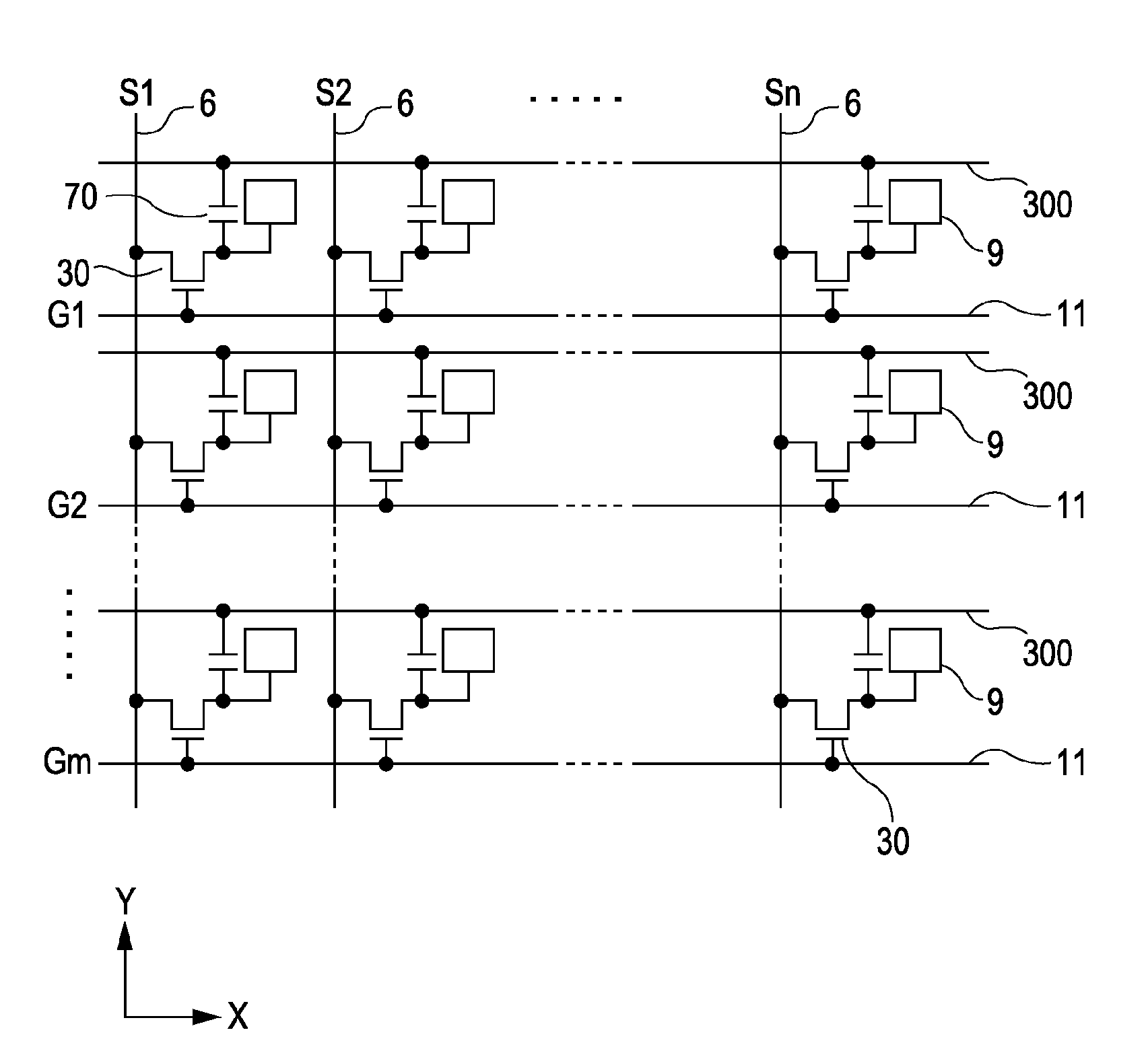
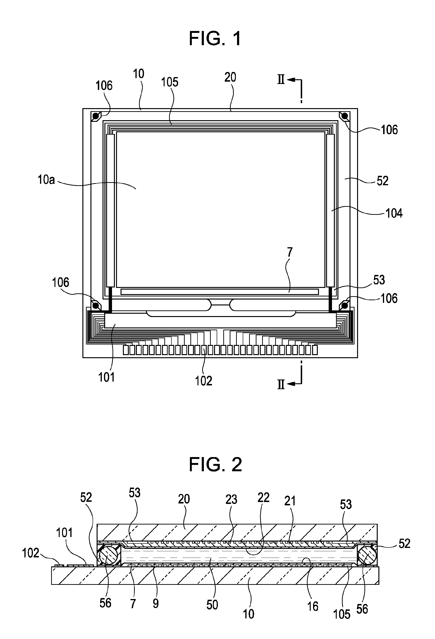
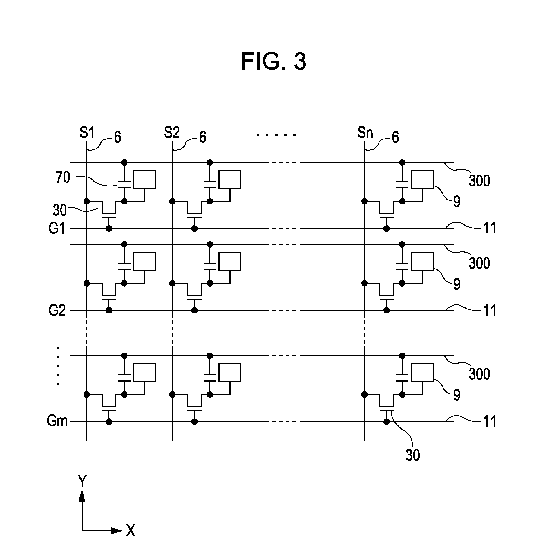
[0059]First, the entire configuration of the liquid crystal device according to the present embodiment will be described with reference to FIGS. 1 and 2.

[0060]FIG. 1 is a schematic plan view showing the configuration of a liquid crystal device when a TFT array substrate 10 is viewed from the side of a counter substrate 20 together with components formed thereon, and FIG. 2 is a cross-sectional view taken along line II-II of FIG. 1.

[0061]In FIGS. 1 and 2, the liquid crystal device according to the present embodiment includes the TFT array substrate 10 and the counter substrate 20 which face each other. The TFT array substrate 10 is, for example, a transparent substrate such as a quartz substrate or a glass substrate or a silicon substrate. The counter substrate 20 is, for example, a transparent substrate such as a quartz substrate or a glass substrate. A liquid crystal layer 50 is filled between the TFT array substrate 10 and the counter substrate 20, and the TFT array substrate 10 a...

second embodiment

[0106]Next, a liquid crystal device according to a second embodiment will be described with reference to FIGS. 10 to 12. The second embodiment is different from the first embodiment in some configurations and is similar in the other configurations. To this end, in the second embodiment, portions different from those of the first embodiment will be described in detail and the description of the overlapping portions will be properly omitted.

[0107]FIGS. 10 and 11 are plan views projectively showing the positional relationship between the layers configuring the liquid crystal device according to the second embodiment. FIG. 12 is a cross-sectional view showing a lamination structure of the liquid crystal device according to the second embodiment. In addition, the layers of the lower layer side of a fourth relay layer 91 and a third relay layer 92 are shown in FIG. 10 and the layers of the upper layer side of the fourth relay layer 91 and the third relay layer 92 are shown in FIG. 11. In ...


PUM


Abstract

Provided is an electro-optical device including: a plurality of pixel electrodes arranged in a pixel region; a lower electrode disposed at a lower layer side of the plurality of pixel electrodes with a dielectric film interposed therebetween so as to at least partially overlap the plurality of pixel electrodes in plan view; and a step difference reduction film disposed on an underlying surface of the lower electrode and formed in at least a portion of a lower electrode non-forming region of the pixel region so as to reduce a step difference between the upper surfaces of the lower electrode and the underlying surface in the lower electrode non-forming region.

Description

BACKGROUND[0001]1. Technical Field[0002]The present invention relates to a technical field of an electro-optical device such as a liquid crystal device and an electronic apparatus such as a liquid crystal projector including the electro-optical device.[0003]2. Related Art[0004]A liquid crystal device which is a kind of electro-optical device is configured by interposing liquid crystal, which is an example of an electro-optical material, between a pair of substrates. On one of the pair of substrates, a lamination structure formed of pixel switching Thin Film Transistors (TFTs) or lines such as scanning lines or data lines is formed, and a plurality of pixel electrodes is provided at an uppermost layer side of the lamination structure in a matrix. In such an electro-optical device, for the purpose of high contrast of a display image, storage capacitors may be provided between the pixel switching TFTs and the pixel electrodes. For example, JP-A-6-148684 discloses a technique of forming...

Claims


Application Information

Patent Timeline
IPC IPC(8): G02F1/1343G02F1/03
CPCG02F1/136227G02F1/136213
Inventor OIKAWA, HIROYUKI
Owner SEIKO EPSON CORP
Why Eureka
Try Eureka