Semiconductor device and display device including the semiconductor device

a display device and semiconductor technology, applied in semiconductor devices, instruments, computing, etc., can solve the problems of reducing the yield affecting the performance of the display device, and generating defects in the connection portion between the wirings in some cases, so as to achieve excellent electrical characteristics and excellent electrical characteristics

Active Publication Date: 2016-03-22
SEMICON ENERGY LAB CO LTD
View PDF138 Cites 4 Cited by
  • Summary
  • Abstract
  • Description
  • Claims
  • Application Information

AI Technical Summary

Benefits of technology

[0010]Another object of one embodiment of the present invention is to give favorable electrical characteristics to a semiconductor device including an oxide semiconductor. Another object is to provide a highly reliable semiconductor device which includes an oxide semiconductor and in which a change in the electrical characteristics is suppressed. Another object of one embodiment of the present invention is to provide a semiconductor device that is suitable for miniaturization. Another object of one embodiment of the present invention is to provide a semiconductor device with high productivity.
[0013]The distance between the upper end portion and the lower end portion of the second wiring is longer than that of each of the source electrode and the drain electrode, whereby a step difference due to the second wiring can be reduced. By reducing the step difference due to the second wiring, the coverage with the insulating films and / or the conductive film, which are formed over the second wiring, can be improved. Thus, a connection portion with excellent electrical characteristics, in other words, with reduced conduction failures can be obtained.
[0014]The distance between the upper end portion and the lower end portion of each of the source electrode and the drain electrode included in the transistor is shorter than that of the second wiring. Such a structure enables the transistor to have favorable electrical characteristics. For example, in the case where the transistor is a channel-etched transistor, at the time of formation of the source electrode and the drain electrode, the oxide semiconductor film, which is a semiconductor layer, might be damaged. However, the source electrode and the drain electrode each have the above structure, whereby damage to the oxide semiconductor film can be minimized. Furthermore, the end portion of each of the source electrode and the drain electrode has the above structure, whereby the electric field can be favorably applied to the oxide semiconductor film serving as a channel region.
[0016]According to one embodiment of the present invention, a semiconductor device including a transistor having excellent electrical characteristics and a connection portion having excellent electrical characteristics can be provided.

Problems solved by technology

In a semiconductor device including an oxide semiconductor film, when transistors and wirings such as a power supply line and a signal line electrically connected to the transistors are integrated with high density, defects are generated in a connection portion between the wirings in some cases.
For example, in the case where the distance between the wirings is narrow, the case where the wiring has a large unevenness of a step, or the like, normal conduction cannot be ensured in the connection portion due to disconnection of a conductive film that connects the wirings or poor coverage of the conductive film that connects the wirings.
In the case where a semiconductor device including such a connection portion is used in a display device, for example, a decrease in the yield of the display device occurs because of malfunction of the connection portion.

Method used


Image

  • Semiconductor device and display device including the semiconductor device
  • Semiconductor device and display device including the semiconductor device
  • Semiconductor device and display device including the semiconductor device

Examples


embodiment 1

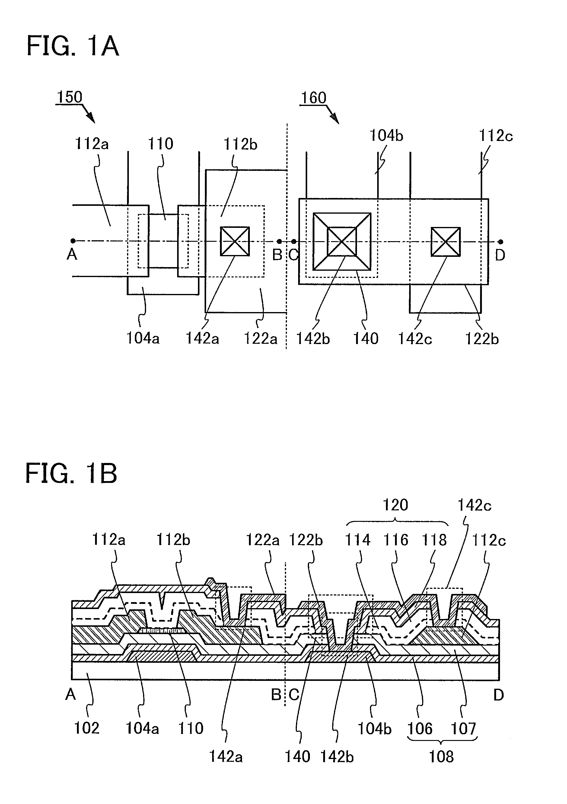
[0043]In this embodiment, a semiconductor device of one embodiment of the present invention is described with reference to FIGS. 1A and 1B, FIGS. 2A to 2D, and FIGS. 3A to 3C.

[0044]FIG. 1A is a top view of the semiconductor device of one embodiment of the present invention, and FIG. 1B is a cross-sectional view taken along a dashed-dotted line A-B and a dashed-dotted line C-D shown in FIG. 1A. Note that in FIG. 1A, some components of the semiconductor device (e.g., an insulating film serving as a gate insulating film) are not illustrated to avoid complexity.

[0045]The semiconductor device in FIGS. 1A and 1B includes a transistor 150 and a connection portion 160.

[0046]The transistor 150 includes a gate electrode 104a over a substrate 102, a first insulating film 108 formed over the gate electrode 104a, an oxide semiconductor film 110 formed in a position over the first insulating film 108 and overlapping with the gate electrode 104a, and a source electrode 112a and a drain electrode 1...

embodiment 2

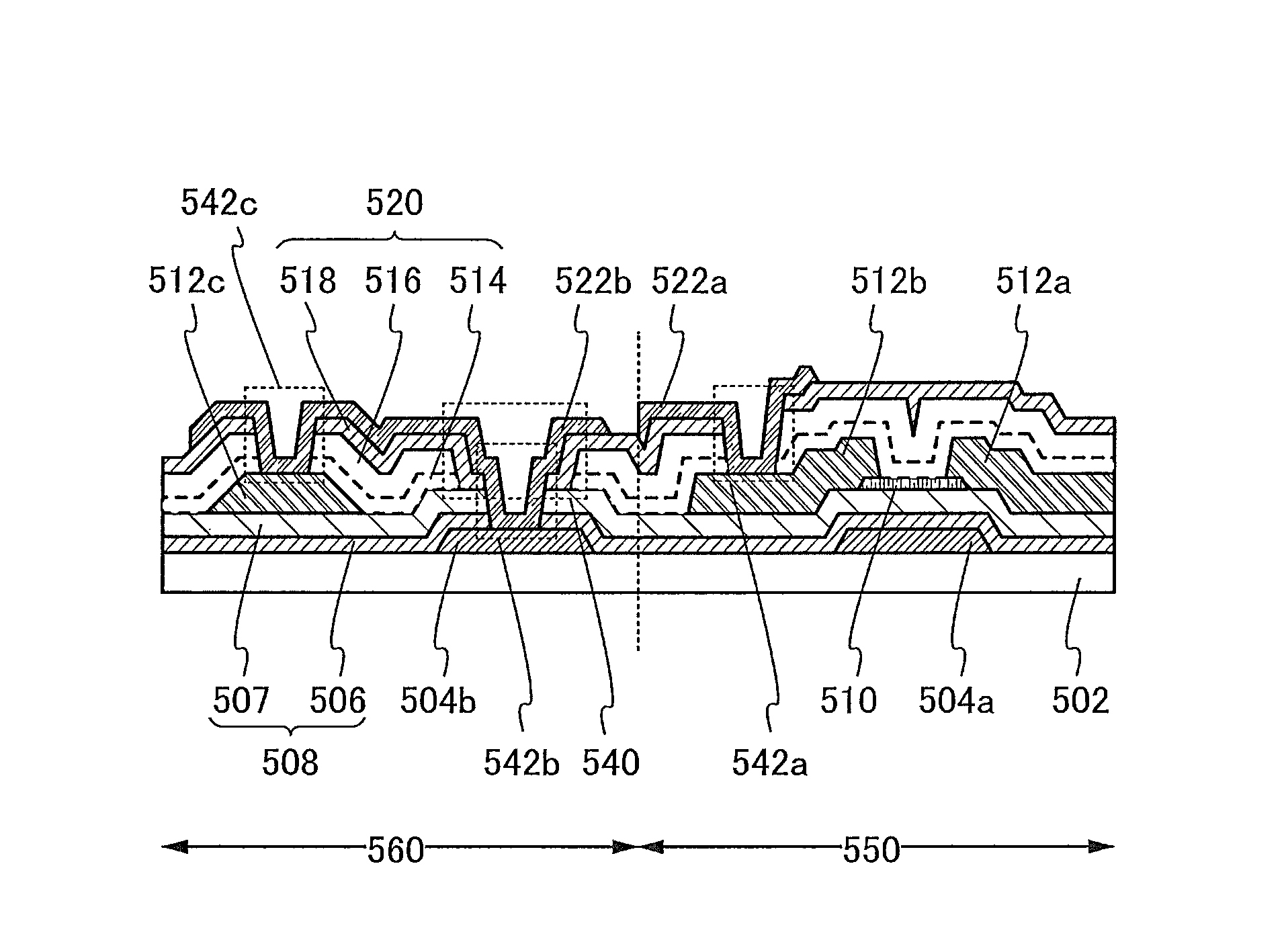
[0172]In this embodiment, a semiconductor device of one embodiment of the present invention is described with reference to FIG. 7, FIGS. 8A to 8D, and FIGS. 9A to 9C. Note that portions similar to those in FIGS. 1A and 1B, FIGS. 2A to 2D, FIGS. 3A to 3C, FIGS. 4A to 4D, FIGS. 5A to 5D, and FIGS. 6A and 6B are denoted by the same reference numerals, and description thereof is omitted.

[0173]A semiconductor device in FIG. 7 is a structural example in which a capacitor 170 is connected to the transistor 150 described in Embodiment 1.

[0174]The transistor 150 includes a gate electrode 104a over a substrate 102, a first insulating film 108 formed over the gate electrode 104a, an oxide semiconductor film 110 formed in a position over the first insulating film 108 and overlapping with the gate electrode 104a, and a source electrode 112a and a drain electrode 112b that are electrically connected to the oxide semiconductor film 110.

[0175]In addition, over the transistor 150, specifically over ...

embodiment 3

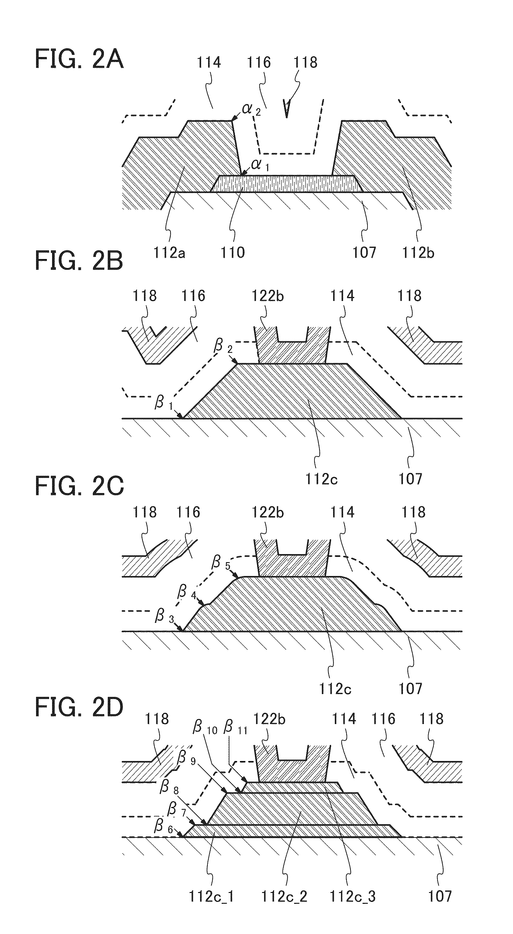
[0203]In this embodiment, a structure of a transistor that can be used in a semiconductor device of one embodiment of the present invention is described with reference to FIGS. 10A and 10B.

[0204]A semiconductor device illustrated in FIG. 10A is an example in which a stack of an oxide semiconductor film 111a and an oxide film 111b is used as the oxide semiconductor film 110 of the transistor 150 included in the above-described semiconductor device. Thus, the other components are the same as those of the transistor 150; hence, the above description can be referred to.

[0205]Here, the oxide semiconductor film 111a and the oxide film 111b are described below in detail.

[0206]Metal oxides used for the oxide semiconductor film 111a and the oxide film 111b preferably contain at least one same constituent element. Alternatively, the constituent elements of the oxide semiconductor film 111a may be the same as those of the oxide film 111b and the composition of the constituent elements of the o...


PUM

PropertyMeasurementUnit
sizeaaaaaaaaaa
temperatureaaaaaaaaaa

Abstract

A semiconductor device including a transistor and a connection portion is provided. The transistor includes a gate electrode, a first insulating film over the gate electrode, an oxide semiconductor film over the first insulating film and at a position overlapping with the gate electrode, and source and drain electrodes electrically connected to the oxide semiconductor film; and the connection portion includes a first wiring on the same surface as a surface on which the gate electrode is formed, a second wiring on the same surface as a surface on which the source and drain electrodes are formed, and a third wiring connecting the first wiring and the second wiring. The distance between an upper end portion and a lower end portion of the second wiring is longer than the distance between an upper end portion and a lower end portion of each of the source and drain electrodes.

Description

BACKGROUND OF THE INVENTION[0001]1. Field of the Invention[0002]The present invention relates to a semiconductor device including a transistor including an oxide semiconductor film. Furthermore, the present invention relates to a display device including the semiconductor device.[0003]2. Description of the Related Art[0004]Attention has been focused on a technique for forming a transistor using a semiconductor thin film formed over a substrate (also referred to as a thin film transistor (TFT)). Such a transistor is used in a wide range of electronic devices such as an integrated circuit (IC) or an image display device (display device). A silicon-based semiconductor material is widely known as a material for a semiconductor thin film applicable to a transistor. As another material, an oxide semiconductor has attracted attention.[0005]For example, a transistor including an oxide semiconductor containing indium (In), gallium (Ga), and zinc (Zn) as an active layer of the transistor has ...

Claims


Application Information

Patent Timeline
Patent Type & Authority Patents(United States)
IPC IPC(8): H01L29/786H01L29/04G02F1/1333H01L27/12
CPCH01L27/1225H01L27/124H01L27/1288H01L27/1248H01L29/7869G02F1/13306G02F1/133345G02F1/13338G02F1/134336G02F1/136286G02F1/1368G02F2201/123G06F3/041G06F2203/04103H01L29/41733H01L29/42384H01L29/4908
Inventor YAMAZAKI, SHUNPEIMIYAKE, HIROYUKISATO, TAKAHIROJINTYOU, MASAMI
Owner SEMICON ENERGY LAB CO LTD
Why Eureka
Try Eureka