Semiconductor device having a modified dielectric film

a technology of dielectric film and semiconductor device, which is applied in the direction of semiconductor device, semiconductor/solid-state device details, electrical apparatus, etc., can solve the problems of reducing the throughput of the manufacturing process of semiconductor device, leaving uncut fuses of such semiconductor device, etc., and achieves the effect of reducing stress

Active Publication Date: 2007-08-09
MICRON TECH INC
View PDF1 Cites 7 Cited by
  • Summary
  • Abstract
  • Description
  • Claims
  • Application Information

AI Technical Summary

Benefits of technology

[0017]In the method of the present invention, the underlying dielectric film formed using the HDP-CVD process, before forming the silicon oxide film, and having the edge in contact with the sidewall of the topmost-layer interconnect lines, increases the corner angle of the silicon oxide film between the bottom surface of the flat part of the silicon oxide film and the bottom surface of the rising part of the silicon oxide film rising on the sidewall of the topmost-layer interconnect lines, compared to the case where the underlying dielectric film is not formed. The larger corner angle allows the portion of the SOG film in the vicinity of the bottom of the topmost-layer interconnect lines to be sufficiently modified, and alleviates the stress applied to the topmost-layer interconnect lines in a later heat treatment.

Problems solved by technology

Thus, some of the fuses of such semiconductor devices may be left uncut.
However, this inevitably reduces the throughput of the process for manufacturing semiconductor devices.

Method used


Image

  • Semiconductor device having a modified dielectric film
  • Semiconductor device having a modified dielectric film
  • Semiconductor device having a modified dielectric film

Examples


Embodiment Construction

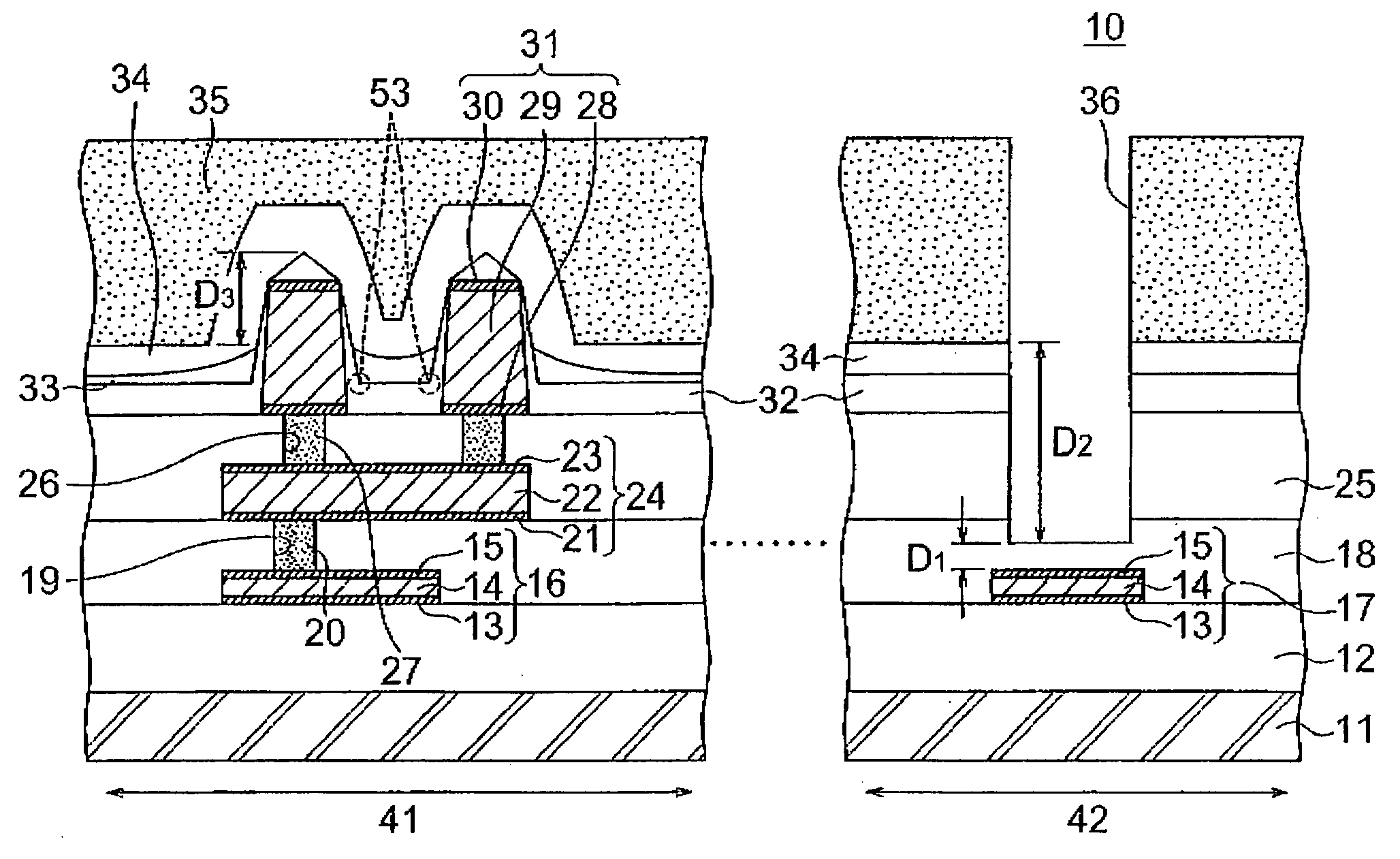
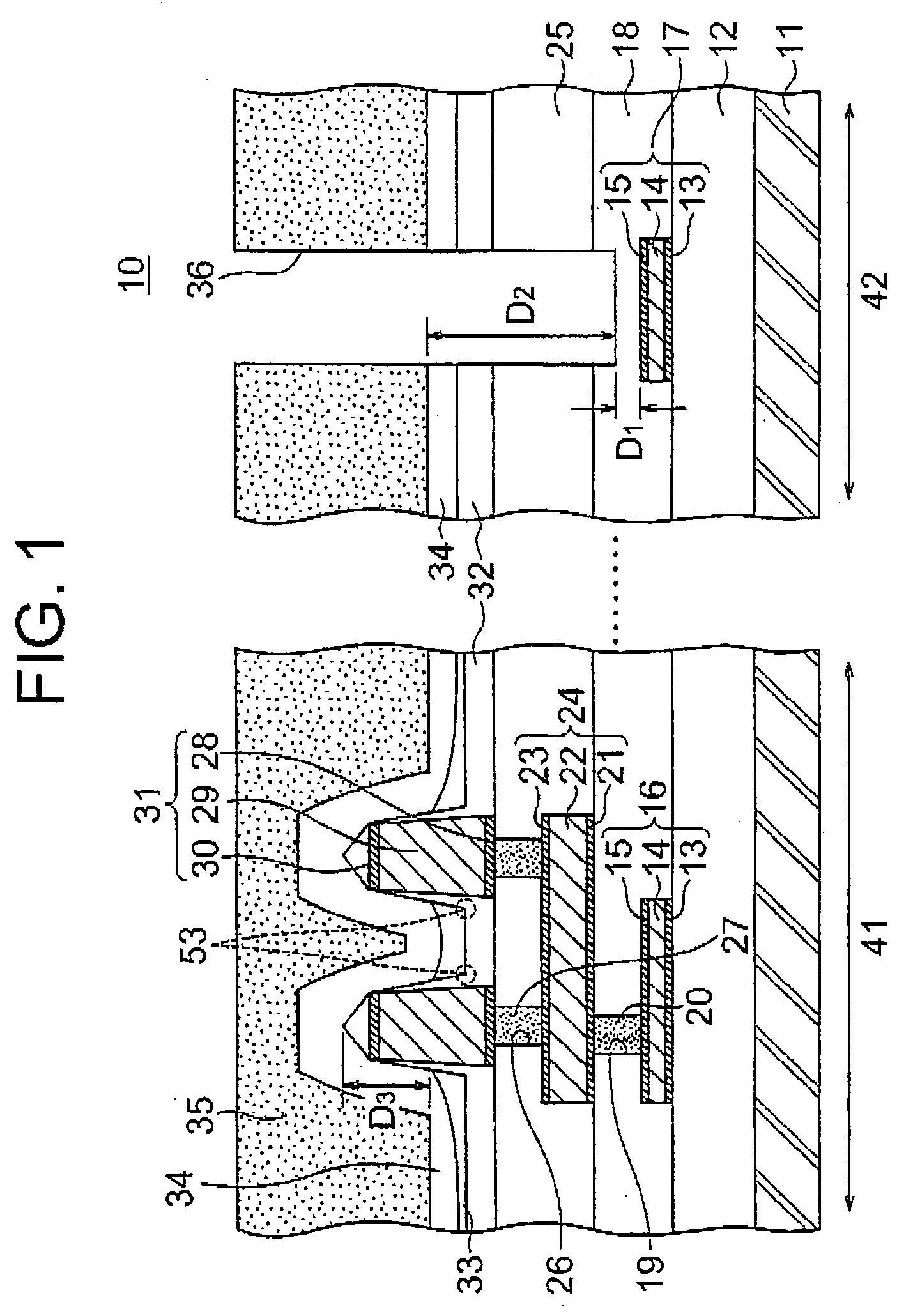
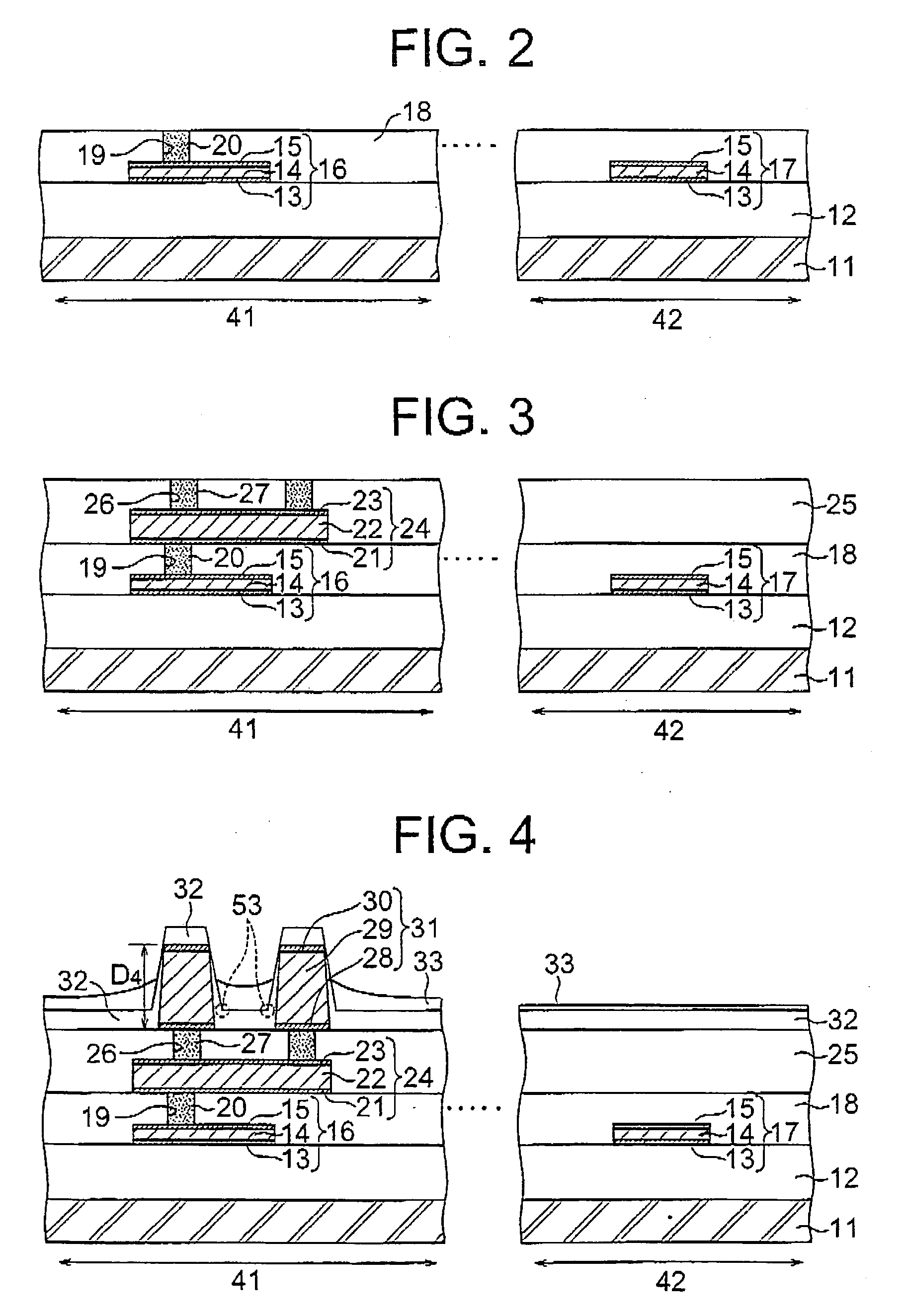
[0027]Now, the present invention will be described in more detail with reference to the accompanying drawings that schematically illustrate preferred embodiments of the invention. FIG. 1 is a schematic sectional view of a semiconductor device according to an embodiment of the present invention, illustrating the structure thereof. Referring to FIG. 1, the semiconductor device 10 is configured as a DRAM device having redundant additional memory cells. FIG. 1 has an element forming region 41 where a memory cell is formed and a fuse forming region 42 where a fuse to be cut by means of a laser beam is formed to control the redundant memory cell, illustrating the respective configurations thereof.

[0028]The semiconductor device 10 includes a semiconductor substrate 11 made of p-type silicon and an interlayer dielectric film 12 formed on the semiconductor substrate 11. The interlayer dielectric film 12 is typically an SiO2 film, a TEOS (tetraethylorthosilicate) film or a BPSG (borophosphosi...


PUM


Abstract

A semiconductor device has a plurality of interconnect layers each including a plurality of interconnect lines. The semiconductor device includes a dielectric film (HDP film) formed by means of high density plasma-enhanced CVD and including an edge formed on the side surface of the topmost-layer interconnect lines, a silicon oxide film formed by modifying a SOG film on the HDP film between adjacent two of the topmost-layer interconnect lines in the element forming region, and a passivation film formed to cover the HDP film and the topmost-layer interconnect lines.

Description

BACKGROUND OF THE INVENTION[0001]1. Field of the Invention[0002]The present invention relates to a semiconductor device having a modified dielectric film and a method of manufacturing the same. More particularly, the present invention relates to a technique suitably applied to a semiconductor device having a laser-cut fuse and a method of manufacturing the same.[0003]2. Description of the Related Art[0004]An aluminum interconnect layer showing a high electric conductivity is used for power supply lines and signal lines formed as upper-layer interconnect lines in a DRAM device, and interconnect lines having a larger thickness have been employed recently from the viewpoint of reducing the access time. Generally, there is a tendency of adding redundant memory cells to DRAM devices for the purpose of accommodating an initial failure of any of the memory cells and a fuse is provided as part of the aluminum interconnect line to control the redundant memory cells. After a device test is co...

Claims


Application Information

Patent Timeline
Patent Type & Authority Applications(United States)
IPC IPC(8): H01L27/108H01L29/00H01L31/036H01L31/112
CPCH01L21/76837H01L23/53223H01L23/5329H01L23/53295H01L2924/0002H01L27/10897H01L2924/12044H01L27/10894H01L2924/00H10B12/09H10B12/50
Inventor ANDO, MASATERU
Owner MICRON TECH INC
Why Eureka
Try Eureka