

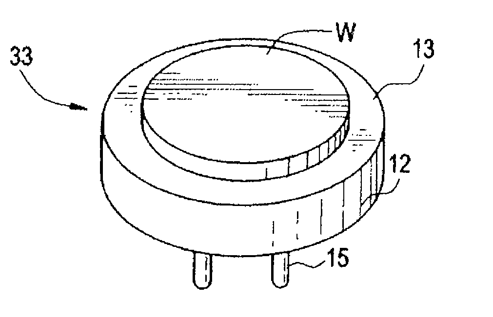
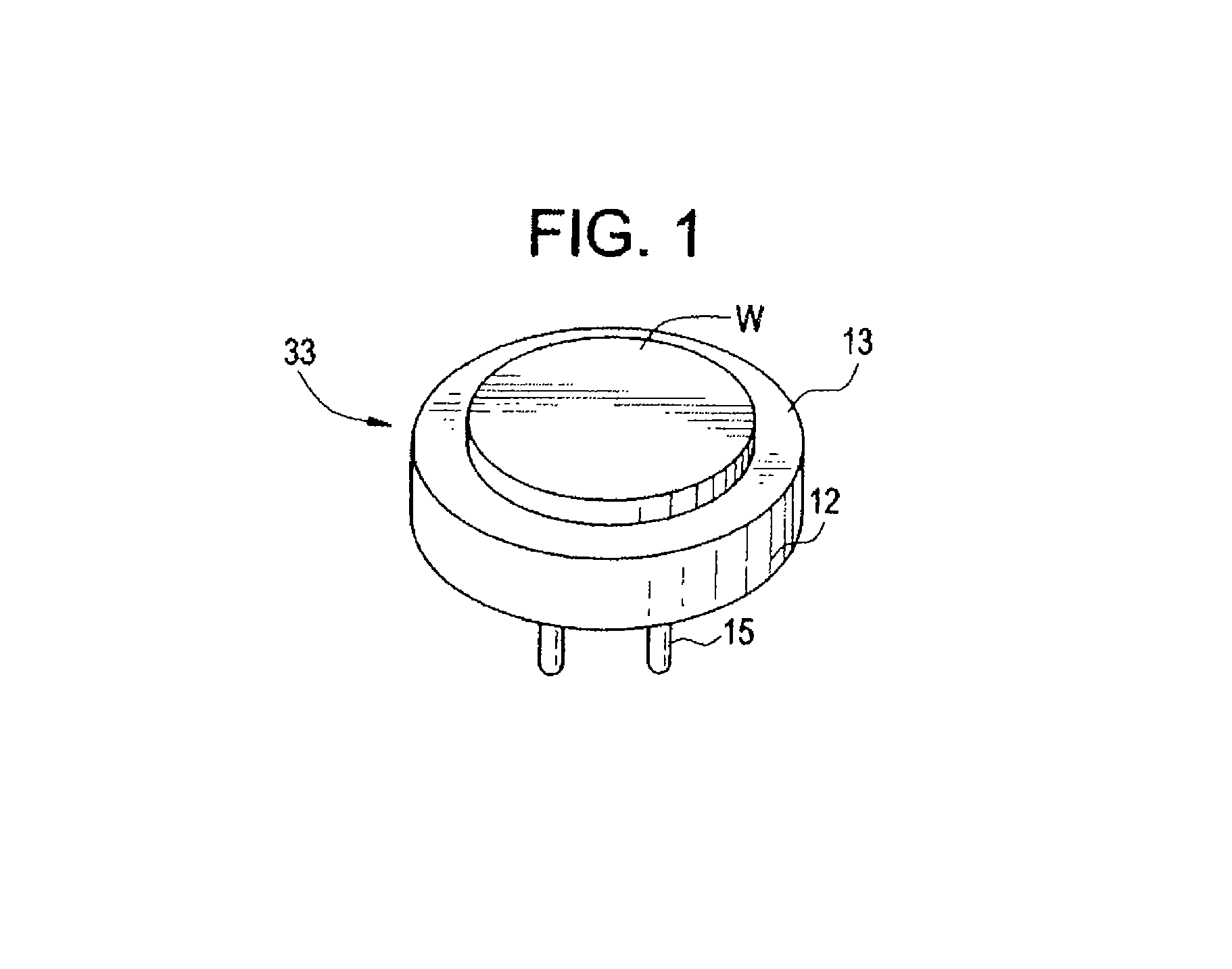
Wafer processing apparatus having a tunable electrical resistivity
a processing apparatus and electrical resistivity technology, applied in the direction of electrical apparatus, basic electric elements, semiconductor/solid-state device manufacturing, etc., can solve the problems of limiting the useful temperature range of a wafer heating apparatus, cumbersome fabrication of chucks, and inability to ramp up the temperature of these types of substrates very quickly
- Summary
- Abstract
- Description
- Claims
- Application Information
AI Technical Summary
Benefits of technology
Problems solved by technology
Method used
Image

Examples
examples
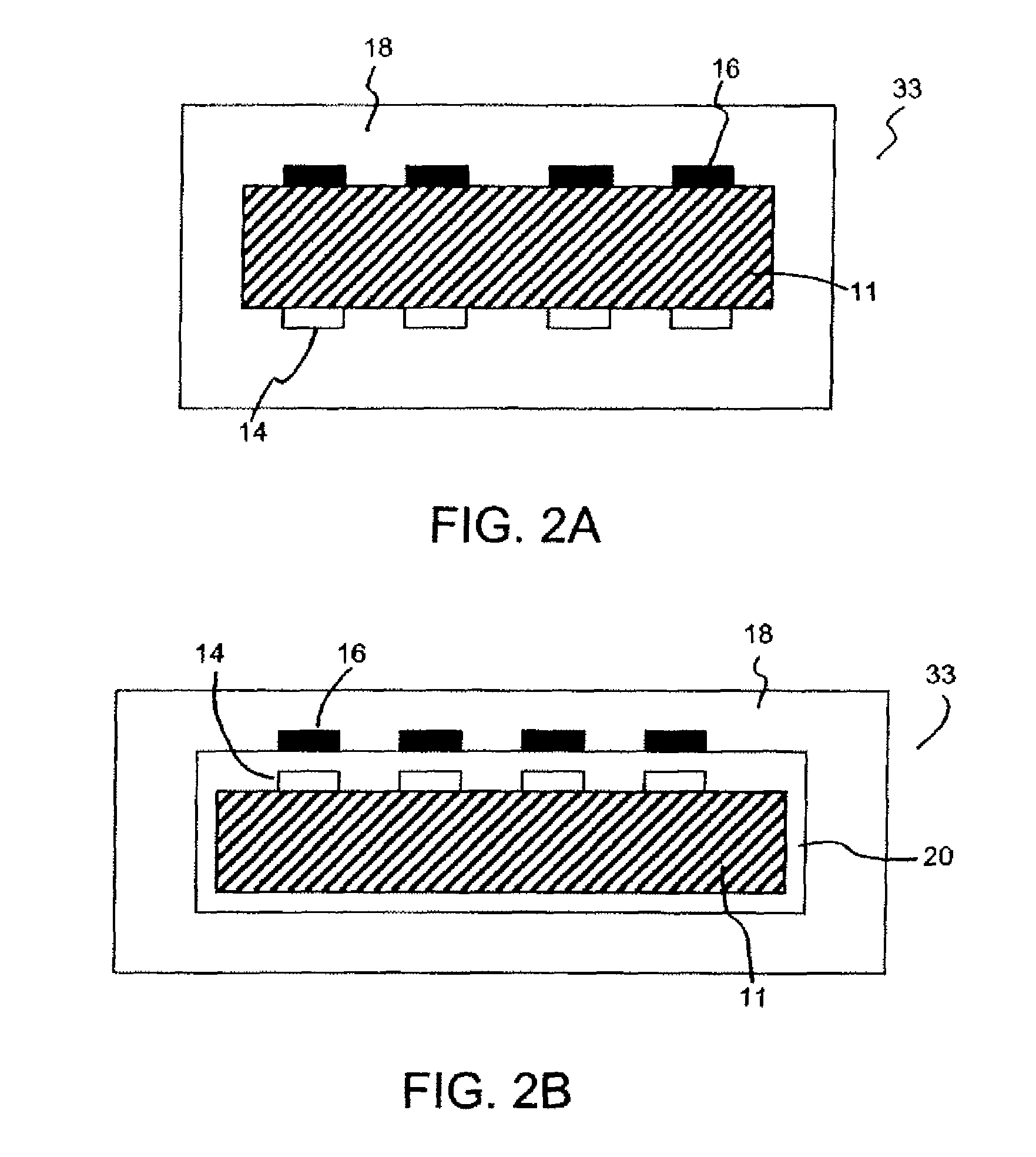
Examples of the layered AlN are shown in Table 1 and in FIG. 8. The examples utilize 3 types of AlN film with varying resistivity. Type-A AlN is a low-density, low resistivity film; Type-B AlN is a high density, mid-range resistivity film; and Type-C AlN is an ultra-high resistivity AlN film. The resistivity measured at 600 C. for each AlN type is shown in Table 1. Sample 70858 consists of 3 layers of AlN, in which layers 1 and 3 are Type-A AlN and layer 2 is Type-B AlN. In this example the composite resistivity of the tri-layer coating falls between the resistivity of the individual layers, and is tuned to 1.5×10⁷ ohm-cm by controlling the thickness of the individual layers. Sample 80153 is a bi-layer structure, in which the resistivity was tuned from 1.3×10¹⁰ ohm-cm, if only Type-C AlN was used, to 4.1×10⁹ ohm-cm. A third example is provided showing the a tri-layer structure utilizing Type-B and Type-C AlN, in which the composite resistivity of the tri-layer structure is tuned to ...
PUM
| Property | Measurement | Unit |
|---|---|---|
| thick | aaaaa | aaaaa |
| temperature | aaaaa | aaaaa |
| temperature | aaaaa | aaaaa |
Abstract
Description
Claims
Application Information