Method of operating nonvolatile memory device

a nonvolatile memory and memory device technology, applied in the field of nonvolatile memory operation, can solve the problems of high operating voltage of the memory device, low dielectric constant of the silicon oxide layer, and insufficient density of the trap site in the silicon nitride layer, etc., to achieve greater stability in programming/erase state, reduce or eliminate the effect of recombination rate and thermalization speed of charges

Active Publication Date: 2011-04-19
SAMSUNG ELECTRONICS CO LTD
View PDF11 Cites 9 Cited by
  • Summary
  • Abstract
  • Description
  • Claims
  • Application Information

AI Technical Summary

Benefits of technology

[0034]Example embodiments provide a method of operating a charge trap flash memory device, which may ensure a greater stability in programming / erase states by improving a thermalization speed of charges and / or a recombination rate of electrons and holes so as to reduce or prevent opposite charges from remaining in a charge trap layer in the programming state or the erase state.

Problems solved by technology

However, in the SONOS memory device having the above structure, the dielectric constants of the silicon nitride layer and the silicon oxide layers are relatively low, and a density of a trap site in the silicon nitride layer may not be sufficient.
Therefore, an operating voltage of the memory device is higher, and a speed of recording data (programming rate) may not be fast enough and charge retention times in vertical and horizontal directions may not be long enough.
However, the electrons injected in an initial programming procedure for an unused CTF memory device may be trapped by the charge trap layer and localized, and then, the electrons may be spatially spread while being thermalized into a deep trap in the nitride layer.
The variation of the time-dependent threshold voltage may Vth make it difficult to control a dispersion of the threshold voltage values when an incremental step pulse programming (ISPP) method is used.
However, if the threshold voltage is changed in time, it may be more difficult to control the dispersion between the threshold voltages using the ISPP method, and it is not easy to program the memory cells to have the threshold voltages within a desired range.
When the thermalization advances further, the change in threshold voltage may be reduced, however, the charges may be localized to a deeper energy level and thus may be more difficult to move.
Therefore, if the recombination takes a long time, the electrons or the holes that are thermalized and localized to the deep energy level according to the elapsed time may not be able to move, and thus, it may be more difficult to recombine the electrons and the holes.
In addition, when the movement of the electrons or the holes is limited due to thermalization, the thermalization time may increase.
In addition, when the recombination time is long, the charges may be thermalized according to the elapsed time, and thus, a sufficient recombination of holes-electrons may not be performed.
Even though a number of electrons are additionally injected, the recombination may be still incomplete and thus the holes may still exist.

Method used


Image

  • Method of operating nonvolatile memory device
  • Method of operating nonvolatile memory device
  • Method of operating nonvolatile memory device

Examples


Embodiment Construction

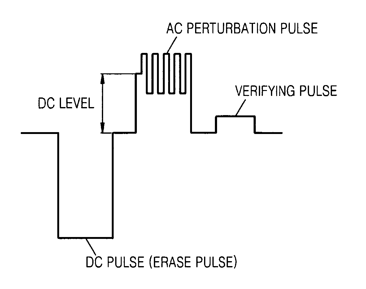
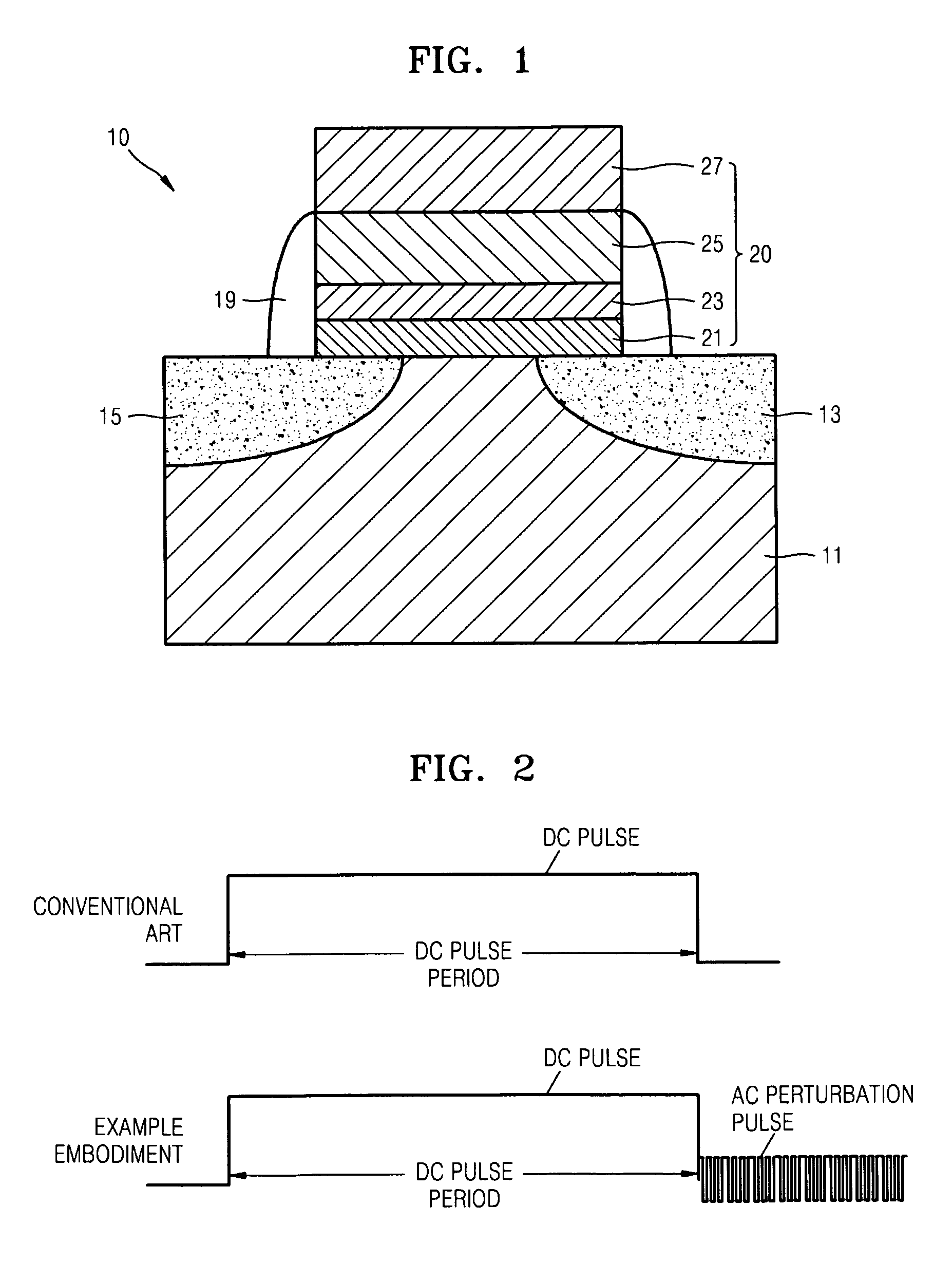
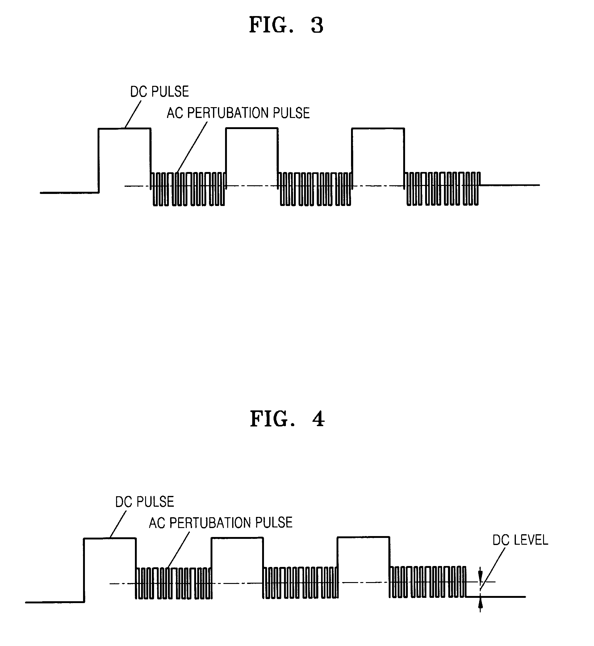
[0068]Reference will now be made in detail to example embodiments, examples of which are illustrated in the accompanying drawings. However, example embodiments are not limited to the embodiments illustrated hereinafter, and the embodiments herein are rather introduced to provide easy and complete understanding of the scope and spirit of example embodiments. In the drawings, the thicknesses of layers and regions are exaggerated for clarity.

[0069]It will be understood that when an element or layer is referred to as being “on,”“connected to” or “coupled to” another element or layer, it may be directly on, connected or coupled to the other element or layer or intervening elements or layers may be present. In contrast, when an element is referred to as being “directly on,”“directly connected to” or “directly coupled to” another element or layer, there are no intervening elements or layers present. Like reference numerals refer to like elements throughout. As used herein, the term “and / or...


PUM


Abstract

Provided is a method of operating a nonvolatile memory device to perform a programming operation or an erase operation. The method includes applying a composite pulse including a direct current (DC) pulse and an AC perturbation pulse to the nonvolatile memory device to perform the programming operation or the erase operation.

Description

PRIORITY STATEMENT[0001]This application claims the benefit of Korean Patent Application No. 10-2007-0020622, filed on Feb. 28, 2007 and 10-2007-37166, filed on Apr. 16, 2007, in the Korean Intellectual Property Office, the disclosure of which is incorporated herein in its entirety by reference.BACKGROUND[0002]1. Field[0003]Example embodiments relate to a method of operating a nonvolatile memory, and more particularly, to a method of operating a nonvolatile memory, which improves the stability of programming and / or erasing states by accelerating charge stabilization and recombination of electrons and holes.[0004]2. Description of the Related Art[0005]Non-volatile memory devices are semiconductor memory devices that can preserve stored data even when the supply of power is cut off.[0006]A structure of a memory cell, that is, a basic element of the non-volatile memory device, varies according to the application fields of the non-volatile memory device.[0007]In the case of NAND flash s...

Claims


Application Information

Patent Timeline
Patent Type & Authority Patents(United States)
IPC IPC(8): G11C11/34
CPCG11C16/349
Inventor SEOL, KWANG-SOOPARK, SANG-JINLEE, SUNG-HOONPARK, SUNG-ILKIM, JONG-SEOB
Owner SAMSUNG ELECTRONICS CO LTD
Why Eureka
Try Eureka