Wireless IC device

a technology of ic devices and wires, applied in the direction of loop antennas, instruments, and the details of semiconductor/solid-state devices, can solve the problems of degrading the module characteristics of the rfid module, increasing the cost of the rfid, and reducing the accuracy of mounting the components, so as to prevent damage, operation failures, breakdown, and reduce the effect of mounting components

Inactive Publication Date: 2011-04-26
MURATA MFG CO LTD
View PDF286 Cites 4 Cited by
  • Summary
  • Abstract
  • Description
  • Claims
  • Application Information

AI Technical Summary

Benefits of technology

[0009]To overcome the problems described above, preferred embodiments of the present invention provides a wireless IC device that prevents damage, operation failures, and breakdown due to static electrical charge and that is capable of operating even when the accuracy of mounting the components is reduced.

Problems solved by technology

Therefore, a highly accurate mounting device is necessary, which results in an increase in the cost of the RFID.
Furthermore, when the accuracy of the mounting of the components is degraded, the module characteristics of the RFID module are also degraded.

Method used


Image

  • Wireless IC device
  • Wireless IC device
  • Wireless IC device

Examples


first preferred embodiment

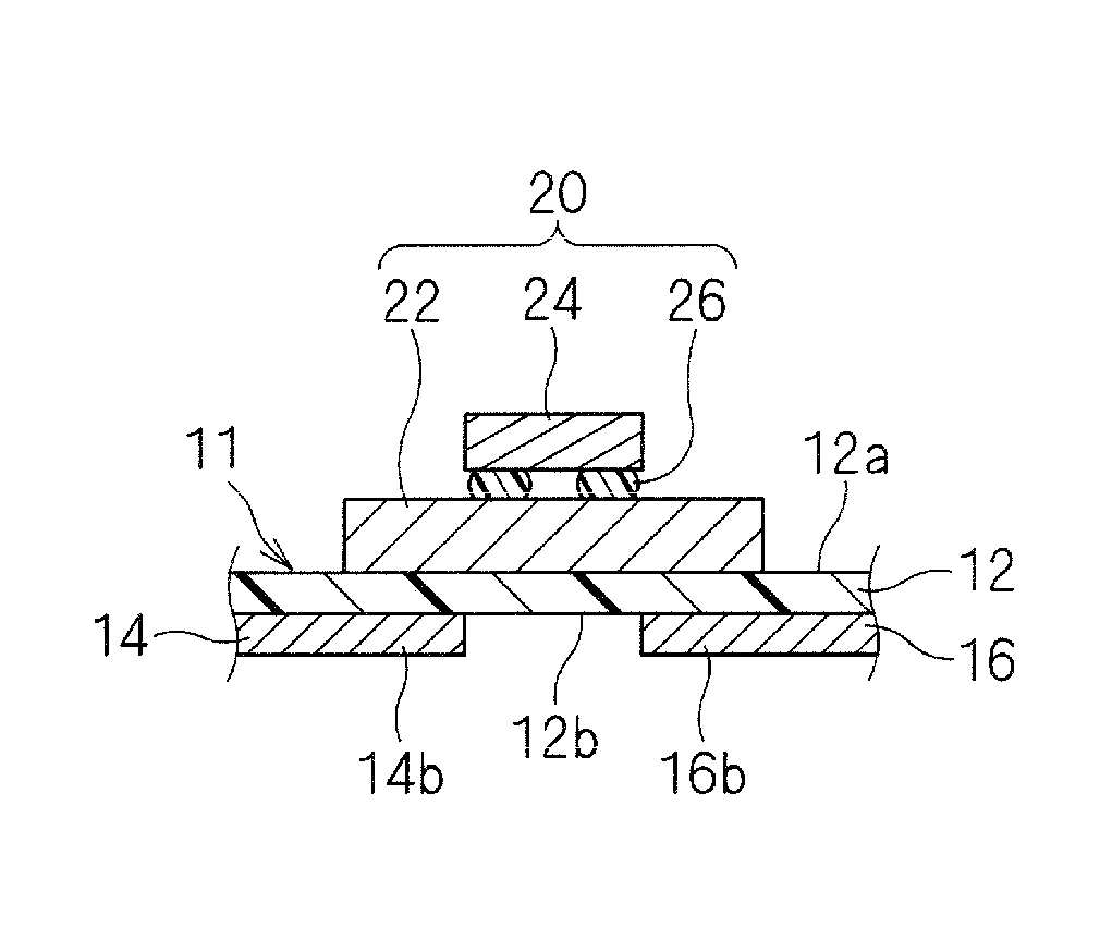
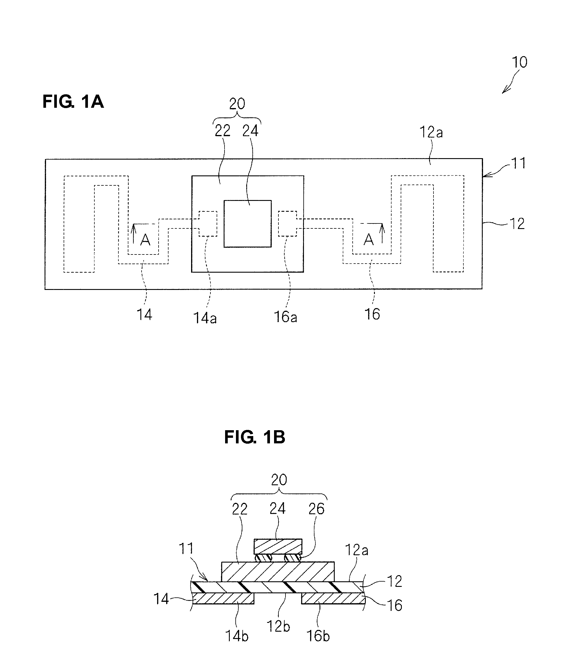
[0040]A wireless IC device according to a first preferred embodiment of the present invention will be described with reference to FIGS. 1A to 3. FIG. 1A is a plan view of a wireless IC device 10. FIG. 1B is a sectional view of a main portion, which is taken along the line A-A in FIG. 1A.

[0041]As illustrated in FIGS. 1A and 1B, the wireless IC device 10 includes an electromagnetic coupling module 20 including a feeding circuit substrate 22 and a wireless IC chip 24. The electromagnetic coupling module 20 is mounted on a top surface 12a, which is one of two main surfaces of a base 12 of a radiation plate 11. The wireless IC device 10 includes radiating electrode patterns 14 and 16 disposed on a bottom surface 12b of the base 12. Alternatively, the radiating electrode patterns may be disposed on the same surface on which the electromagnetic coupling module 20 is mounted.

[0042]The wireless IC device 10 is used by bonding the bottom surface 12b of the base 12 of the radiation plate 11 to...

second preferred embodiment

[0055]In a wireless IC device according to a second preferred embodiment of the present invention, an electromagnetic coupling module 20a is configured as illustrated in a sectional view of a main portion in FIG. 4.

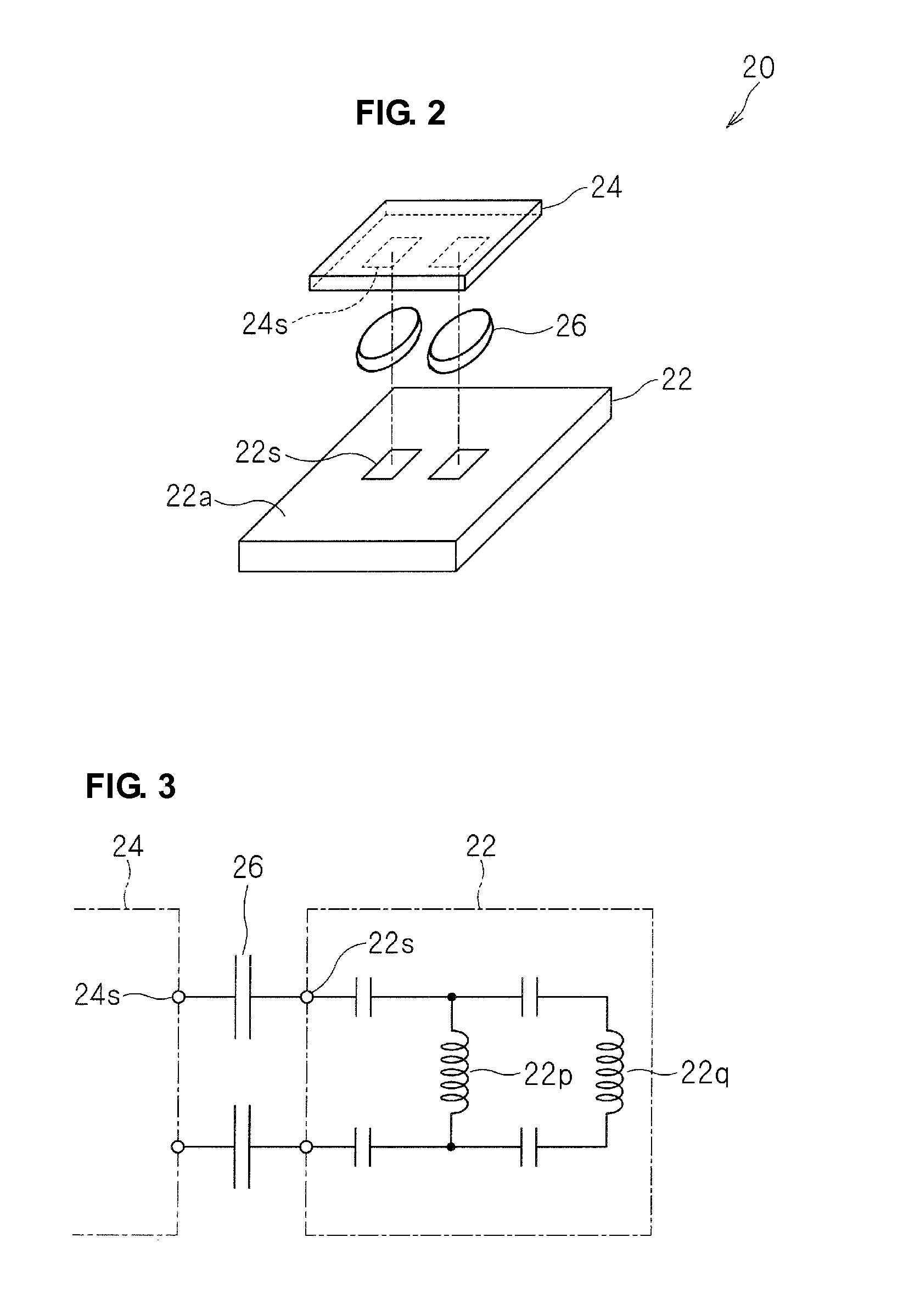
[0056]That is, a dielectric body 26a is disposed on substantially the entire surface 22a of the feeding circuit substrate 22, which is on a side on which the wireless IC chip 24 is disposed. Since only a portion of the dielectric body 26a disposed between the mounting electrode 22s of the feeding circuit substrate 22 and the terminal electrode 24s of the wireless IC chip 24 establishes the capacity coupling, the dielectric body 26a may protrude from a portion that is required for capacity coupling.

[0057]The area of the dielectric body 26a is increased to substantially the size of the wireless IC chip 24, e.g., about 1000 μm2, or greater, and accordingly, the dielectric body 26a can be easily formed.

[0058]Since the dielectric body 26a is arranged in substantially the entir...

third preferred embodiment

[0059]In a wireless IC device according to a third preferred embodiment of the present invention, an electromagnetic coupling module 20b is configured as illustrated in a sectional view of a main portion in FIG. 5.

[0060]A dielectric body 26b preferably made of a mold resin, for example, is arranged along a periphery of the wireless IC chip 24. In a state in which the wireless IC chip 24 is covered with the dielectric body 26, the wireless IC chip 24 is mounted on the feeding circuit substrate 22. Since the wireless IC chip 24 is covered with the dielectric body 26b, entry of dirt, debris, water, moisture or other liquid, for example, into the wireless IC chip 24 is effectively prevented.


PUM


Abstract

A wireless IC device includes a radiation plate, a feeding circuit substrate on which a feeding circuit including a resonant circuit including an inductance element is provided, the feeding circuit being electromagnetically coupled to the radiation plate, and a wireless IC chip including a connection electrode, the wireless IC chip being disposed on the feeding circuit substrate. A mounting electrode is provided on the feeding circuit substrate. The frequency of signals sent and received using the radiation plate substantially corresponds to the resonant frequency of the resonant circuit. The wireless IC chip is electromagnetically coupled to the mounting electrode.

Description

BACKGROUND OF THE INVENTION[0001]1. Field of the Invention[0002]The present invention relates to wireless IC devices, and more specifically, to a wireless IC device, such as a contactless IC medium module used in, for example, an RFID (Radio Frequency Identification) system.[0003]2. Description of the Related Art[0004]Various wireless IC devices including a wireless IC chip and a radiation plate have been proposed.[0005]For example, a contactless IC medium module (RFID) disclosed in Japanese Unexamined Patent Application Publication No. 2003-331246 includes, as illustrated in FIG. 7A which is a top view and FIG. 7B which is a sectional view taken along the line A-A′ in FIG. 7A, an insulating substrate 106 on which a loop antenna 102 and one electrode 101 are provided. Another electrode 103 includes a capacitor defined by electrically conductive wires 115 including insulating films. A resonant circuit including the capacitor and the loop antenna 102 is connected to an LSI 104(Large S...

Claims


Application Information

Patent Timeline
Patent Type & Authority Patents(United States)
IPC IPC(8): G06K19/06
CPCG06K19/07749H01Q7/00H01Q1/2208G06K19/07756H01L2224/16225
Inventor KATO, NOBORUDOKAI, YUYAIKEMOTO, NOBUO
Owner MURATA MFG CO LTD
Why Eureka
Try Eureka