Wafer calibration device and semiconductor processing equipment

A wafer calibration, wafer technology, applied in semiconductor/solid-state device manufacturing, electrical components, circuits, etc., can solve the problems of large data processing and calibration of processing units, increase the difficulty of implementation, increase hardware costs, etc., to reduce equipment and Production cost, burden reduction, effect of production cost reduction

Inactive Publication Date: 2015-11-25
BEIJING NAURA MICROELECTRONICS EQUIP CO LTD
View PDF5 Cites 7 Cited by
  • Summary
  • Abstract
  • Description
  • Claims
  • Application Information

AI Technical Summary

Problems solved by technology

The existence of the transition region makes it necessary to search for the real light-dark junction in the subsequent data processing process, that is, to obtain the actual edge position information of the wafer, thus bringing a greater burden on the data processing and calibration of the processing unit
Moreover, since the longer the length of the transition zone, the higher the requirement for the optimization degree of the processing unit, this not only increases the difficulty of implementation, but also increases the hardware cost
[0008] Second, in theory, only when the light receiving assembly 12 is absolutely parallel to the surface of the wafer, and the light emitted by the light source is parallel light, the transition zone can be avoided. To achieve this, the installation accuracy and calibration accuracy of the wafer alignment device must be raised. higher requirements, thereby increasing production costs

Method used


Image

  • Wafer calibration device and semiconductor processing equipment
  • Wafer calibration device and semiconductor processing equipment
  • Wafer calibration device and semiconductor processing equipment

Examples


Embodiment Construction

[0030] In order for those skilled in the art to better understand the technical solution of the present invention, the wafer alignment device and semiconductor processing equipment provided by the present invention will be described in detail below in conjunction with the accompanying drawings.

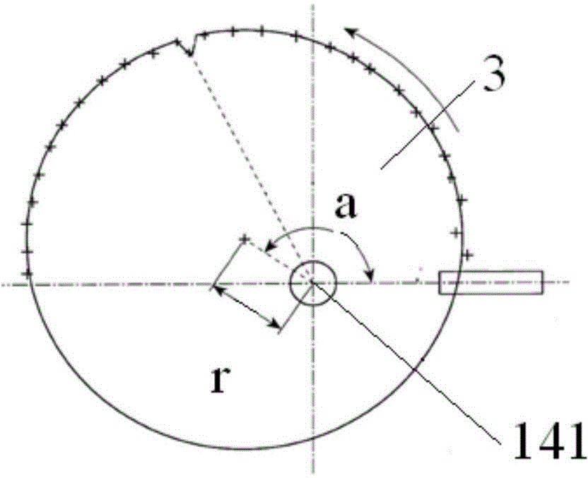
[0031] Figure 4A It is a sectional view of the wafer alignment device provided by the first embodiment of the present invention. Figure 4B for along Figure 4A Sectional view of line A-A. Please also refer to Figure 4A and 4B , the wafer alignment device includes a vacuum chamber 20, a carrier, a rotating mechanism, a light source 23, and a light receiving and processing device. Wherein, the carrier includes a rotating platform 22 and three supporting columns 21, wherein the rotating platform 22 is arranged in the vacuum chamber 20; the three supporting columns 21 are fixed on the rotating platform 22, and are distributed at intervals along its circumference; and, The tops of ...


PUM


Abstract

The invention provides a wafer calibration device and semiconductor processing equipment. The wafer calibration device comprises a vacuum chamber, a load bearing member, a rotating mechanism, a light source and a light receiving and processing device, wherein the load bearing member is arranged in the vacuum chamber, and comprises a load bearing surface used for bearing a wafer; the rotating mechanism is used for driving the load bearing member to rotate; the light source is arranged above the load bearing member and used for transmitting light towards the edge of the load bearing surface; the light receiving and processing device comprises a light receiving assembly, and is used for receiving the light, converting the light into electric signals and sending out the electric signals; and the light receiving assembly is arranged below the load bearing surface in the vacuum chamber, and is located close to the position of the load bearing surface. The wafer calibration device provided by the invention can shorten the length of a transition area, thereby not only being capable of reducing the implementation difficulty of software and the hardware cost, but also being capable of reducing requirements for the installation accuracy and the calibration accuracy, and thus being capable of reducing the production cost.

Description

technical field [0001] The invention relates to the technical field of semiconductor processing, in particular to a wafer alignment device and semiconductor processing equipment. Background technique [0002] In the semiconductor manufacturing process, it is necessary to gradually transfer the wafer to be processed from the atmosphere to a vacuum chamber for processes such as etching and deposition. This requires a wafer transfer system consisting of a series of atmospheric equipment and vacuum equipment. For example, it is usually necessary to use a manipulator to carry out the operations of transferring, picking up and placing the wafers, so as to realize the transfer, loading and unloading of the wafers. In order to ensure the stability of the process, it is required that the wafer can be accurately transferred to the designated position. Although the theoretical transfer accuracy of the current manipulator can meet the process requirements, in the actual transfer proces...

Claims


Application Information

Patent Timeline
Patent Type & Authority Applications(China)
IPC IPC(8): H01L21/67H01L21/673
Inventor 李靖
Owner BEIJING NAURA MICROELECTRONICS EQUIP CO LTD
Why Eureka
Try Eureka