Flip chip bump structure and fabrication method

a chip bump and flip chip technology, applied in the field of flip chip bump structure and fabrication methods, can solve the problems of limiting the use of a smd sop process for high density substrates, the inability of the solder screen process to reliably fill the opening of the solder mask, and the inability to reliably use the solder screen process. achieve the effect of small pitch

Active Publication Date: 2011-04-26
AMKOR TECH SINGAPORE HLDG PTE LTD
View PDF20 Cites 198 Cited by
  • Summary
  • Abstract
  • Description
  • Claims
  • Application Information

AI Technical Summary

Benefits of technology

[0007]A method includes forming a patterned buildup layer on a first surface of a dielectric layer, the patterned buildup layer including a patterned buildup layer opening exposing a trace coupled to the dielectric layer. A conductor layer is flash plated on the patterned buildup layer and within the patterned buildup layer opening. An upper resist is formed with a flip chip bump opening

Problems solved by technology

However, if the size of the pads and thus solder mask openings becomes too small, i.e., the bump pitch becomes too small, the solder screen process cannot be reliably used to fill the soldermask openings.
Unfortunately, this limits the use

Method used


Image

  • Flip chip bump structure and fabrication method
  • Flip chip bump structure and fabrication method
  • Flip chip bump structure and fabrication method

Examples


Embodiment Construction

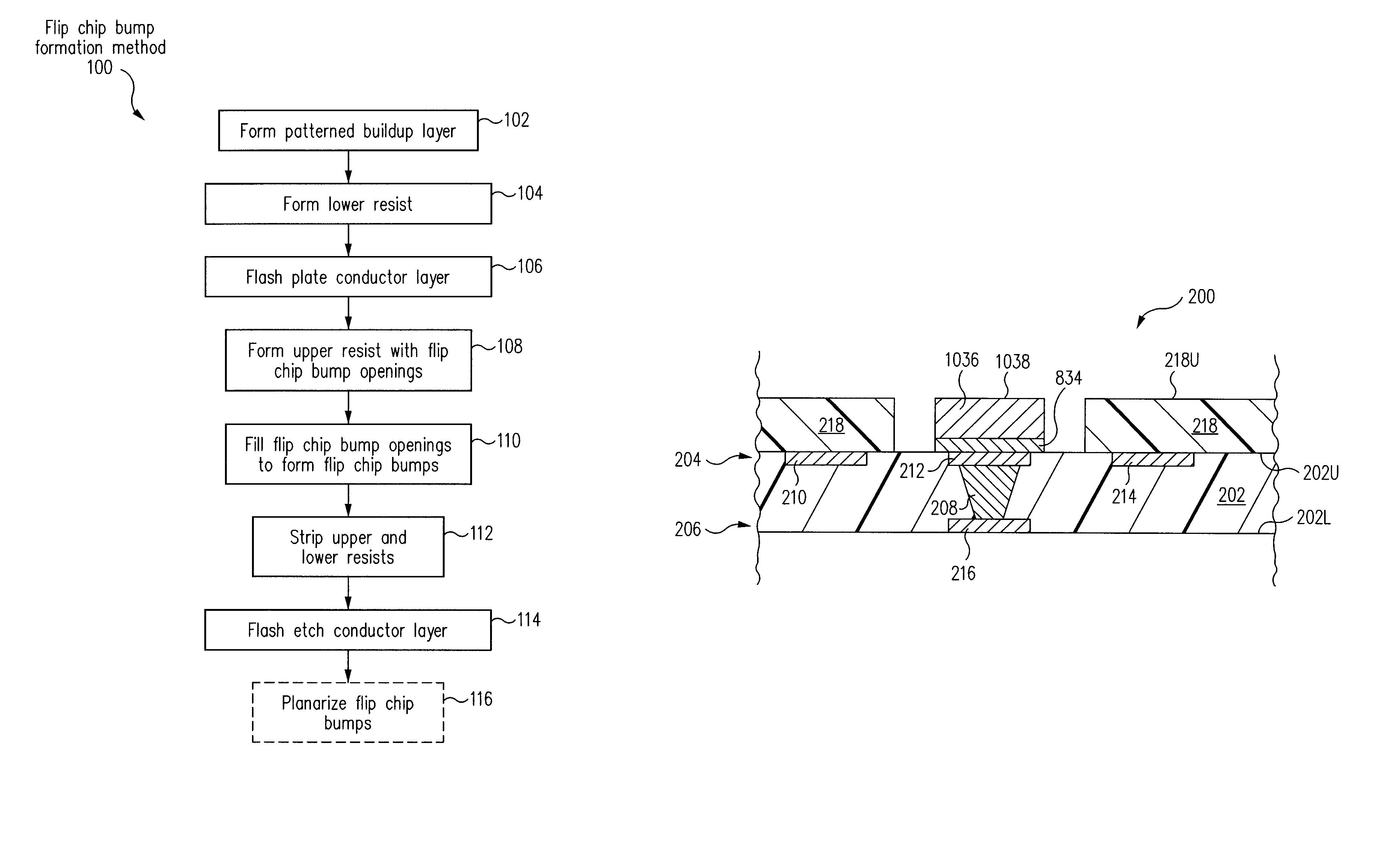
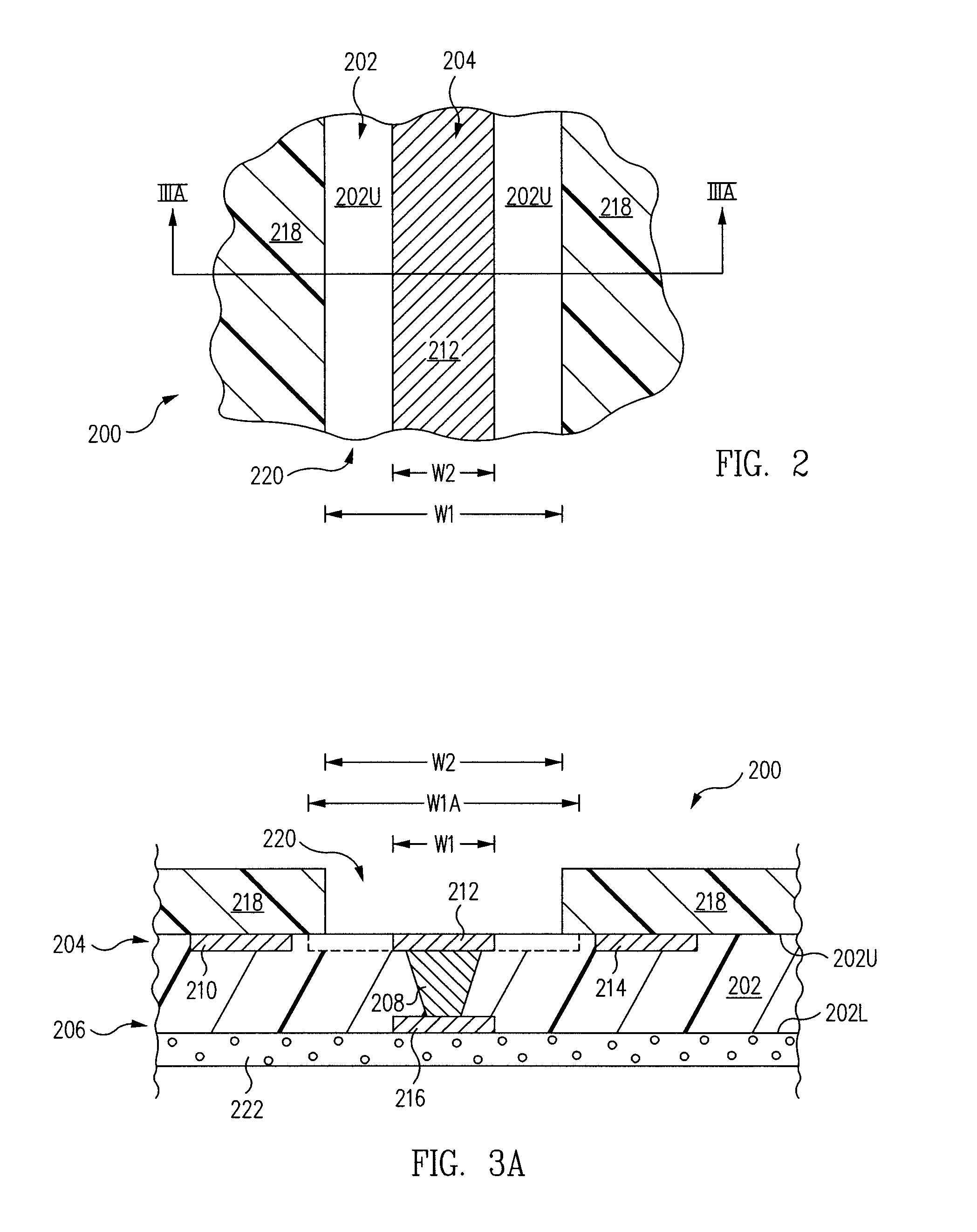
[0038]Referring to FIGS. 1, 2 and 3A together, a flip chip bump formation method 100 includes forming a patterned buildup layer 218 on a first surface 202U of a dielectric layer 202, patterned buildup layer 218 including a patterned buildup layer opening 220 exposing a trace 212 coupled to dielectric layer 202 in a form patterned buildup layer operation 102.

[0039]Referring now to FIGS. 1 and 4 together, a conductor layer 424 is flash plated on patterned buildup layer 218 and within patterned buildup layer opening 220 in a flash plate conductor layer operation 106.

[0040]Referring now to FIGS. 1, 5, and 6 together, a patterned upper resist 526 is formed with a flip chip bump opening 528 that exposes a portion of conductor layer 424 above trace 212 in a form upper resist with flip chip bump openings operation 108.

[0041]Referring now to FIGS. 1, 6 and 7 together, flip chip bump opening 528 is filled to form a flip chip bump 630 in a fill flip chip bump openings to form flip chip bumps o...


PUM


Abstract

A method includes forming a patterned buildup layer on a first surface of a dielectric layer, the patterned buildup layer including a patterned buildup layer opening exposing a trace coupled to the dielectric layer. A conductor layer is flash plated on the patterned buildup layer and within the patterned buildup layer opening. The patterned buildup layer opening is filled with a blanket conductive filler layer. The blanket conductive filler layer and the conductor layer are planarized to form a flip chip bump.

Description

BACKGROUND OF THE INVENTION[0001]1. Field of the Invention[0002]The present application relates to the field of electronics, and more particularly, to methods of forming flip chip bumps and related structures.[0003]2. Description of the Related Art[0004]A Solder On Pad (SOP) process is a technique of applying solder directly to an electrically conductive pad of a substrate to form a flip chip bump thereon. A SOP process encompasses both a solder mask defined (SMD) SOP process and a non solder mask defined (NSMD) SOP process.[0005]In a SMD SOP process, openings are formed in a soldermask. Electrically conductive pads of the substrate are exposed through the soldermask openings. A solder screen process is used to apply solder paste within the soldermask openings. The solder paste is ref lowed (heated to a melt and then cooled) to form flip chip bumps in the soldermask openings and electrically connected to the pads. However, if the size of the pads and thus solder mask openings become...

Claims


Application Information

Patent Timeline
IPC IPC(8): H01L21/44
CPCH01L21/4853H01L24/16H01L2924/14H01L2924/01079H01L2924/01078H01L2224/13021H01L2224/1147
Inventor HUEMOELLER, RONALD PATRICKST. AMAND, ROGER D.DARVEAUX, ROBERT FRANCIS
Owner AMKOR TECH SINGAPORE HLDG PTE LTD
Why Eureka
Try Eureka