Memory card and method for manufacturing memory card

a memory card and manufacturing method technology, applied in the field of memory cards and manufacturing methods, can solve the problems of reducing the thickness of the memory card disclosed in the patent document 1, affecting the appearance of the supposed area, and the structure of the memory card in construction, so as to achieve the effect of thin memory card and simplified memory card in construction

Inactive Publication Date: 2011-05-10
PANASONIC CORP
View PDF13 Cites 10 Cited by
  • Summary
  • Abstract
  • Description
  • Claims
  • Application Information

AI Technical Summary

Benefits of technology

[0016]The foregoing structure allows simplifying the memory card in construction and achieving the smaller as well as the thinner memory card.
[0022](e) covering the first semiconductor chip and the second semiconductor chip with a cover disposed over the principal face of the circuit board.The foregoing method allows manufacturing the memory card excellent in productivity and reliability and having a smaller and a thinner body.

Problems solved by technology

However, the memory card disclosed in patent document 1 is limited to decrease its thickness because the memory chips are layered together.
This structure also complicates the memory card in construction.
However, the foregoing flip-chip mounting method has the following problems: When a semiconductor chip is urged against a circuit board, the resin beneath the semiconductor chip spreads over the surrounding of the chip, and hardens in this state.
As a result, it is difficult to mount this another semiconductor chip to the supposed area.
As discussed above, it is difficult to mount the semiconductor chips as close as possible, e.g. not greater than 1 mm between each semiconductor chip, so that the memory card is limited to be smaller.

Method used


Image

  • Memory card and method for manufacturing memory card
  • Memory card and method for manufacturing memory card
  • Memory card and method for manufacturing memory card

Examples


first exemplary embodiment

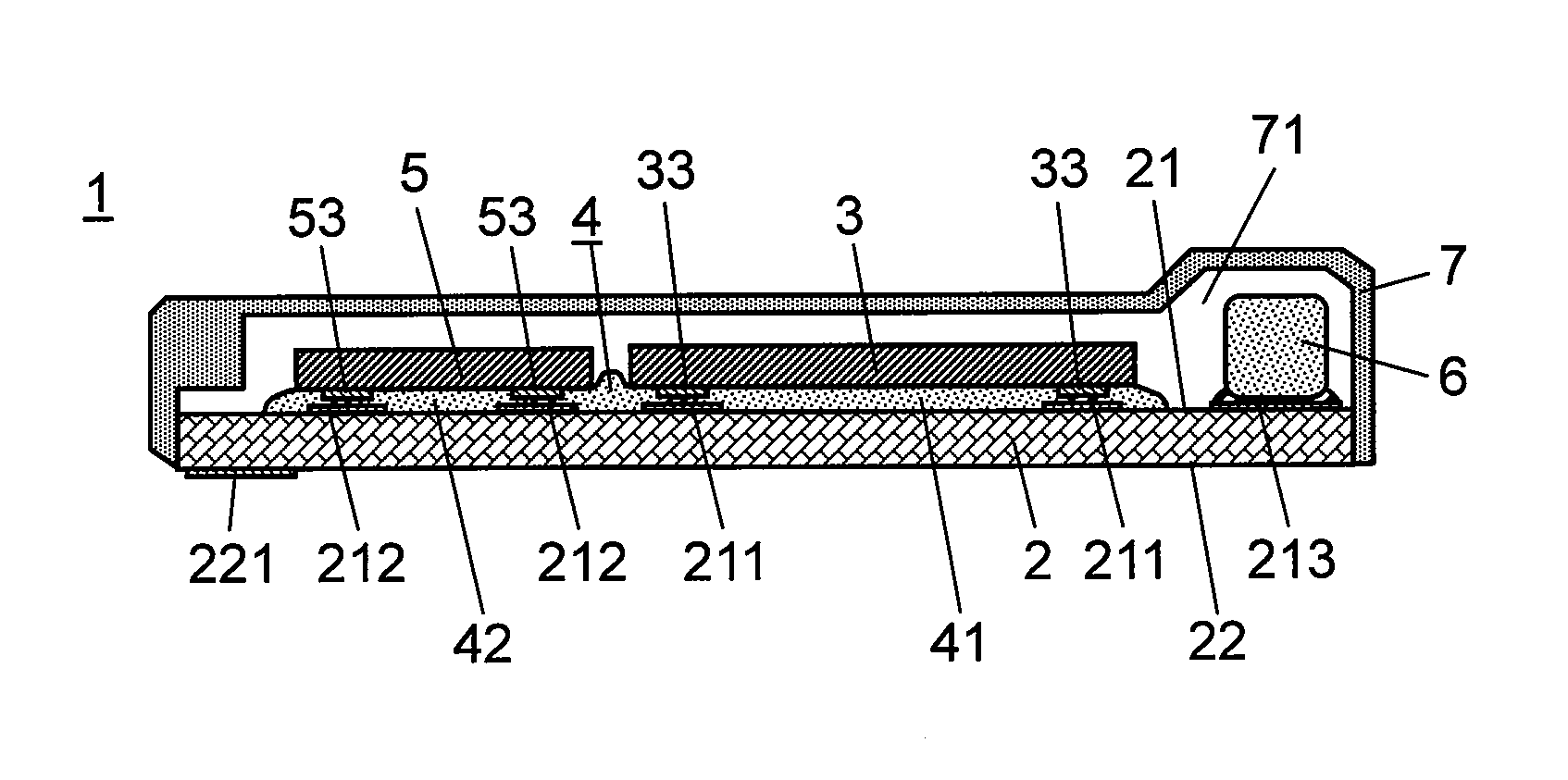
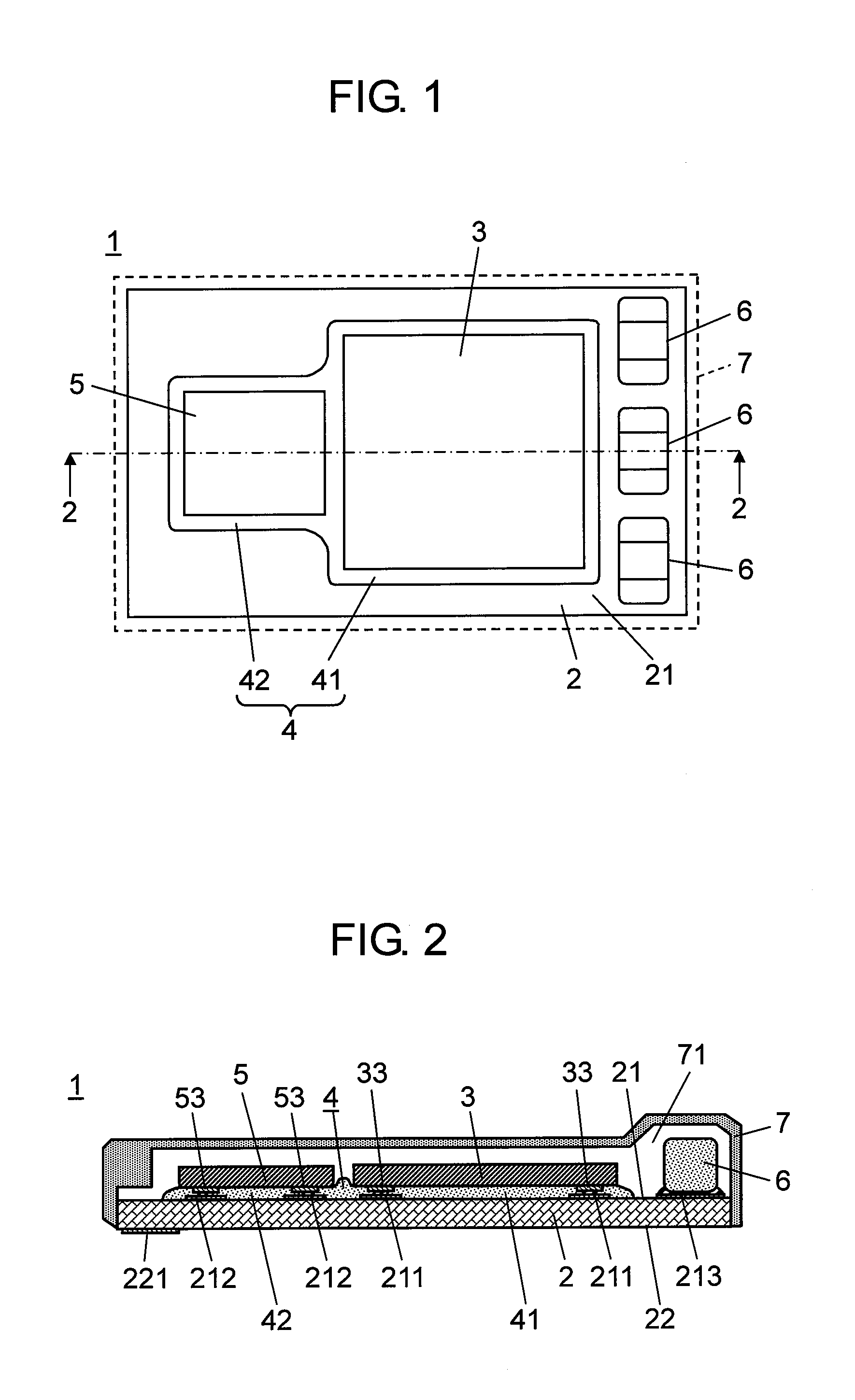
[0057]FIG. 1 shows a plan view illustrating a structure of memory card 1 in accordance with the first exemplary embodiment of the present invention. FIG. 2 shows a sectional view of memory card 1 shown in FIG. 1 cut along line 2-2. In FIG. 1, cover 7 is shown only its outline with dotted lines in order to show the interior structure of memory card 1 more clearly. The covers shown in FIG. 5, FIG. 7 and FIG. 8 are drawn in a similar way.

[0058]In this exemplary embodiment, memory card 1 employs an SD memory card (Secure Digital memory card). Memory card 1 has the following typical dimensions:

[0059]Length: between 14.9 mm and 15.1 mm, (horizontal direction in FIG. 1)

[0060]Width: between 10.9 mm and 11.1 mm (vertical direction in FIG. 1)

[0061]Thickness: between 0.9 mm and 1.1 mm. (vertical direction in FIG. 2)

[0062]For a convenient purpose of description, an upper side and a lower side in FIG. 2 are referred to as an upper side and a lower side of memory card 1. In the exemplary embodime...

second exemplary embodiment

[0091]A memory card in accordance with the second exemplary embodiment of the present invention is demonstrated hereinafter with reference to FIGS. 5 and FIG. 6. FIG. 5 shows a plan view illustrating a structure of memory card 1a in accordance with the second exemplary embodiment, and FIG. 6 shows a sectional view of memory card 1a shown in FIG. 5 cut along line 6-6.

[0092]As shown in FIG. 5 and FIG. 6, memory card 1a includes third semiconductor chip 8, such as a memory chip, mounted on top face 21 of circuit board 2 with bump 83 sandwiched between third semiconductor chip 8 and circuit board 2, in addition to the structure of memory card 1 shown FIGS. 1 and 2. Other structures remain unchanged from those shown in FIGS. 1 and 2, and they have the same reference marks in FIGS. 5 and 6.

[0093]Memory card 1a includes first semiconductor chip 3, second semiconductor chip 5, and third semiconductor chip 8 disposed linearly on top face 21 of circuit board 2. Third semiconductor chip 8 is p...

third exemplary embodiment

[0103]A memory card in accordance with the third exemplary embodiment of the present invention is demonstrated hereinafter with reference to FIG. 8 and FIG. 9. FIG. 8 shows a plan view illustrating a structure of memory card 1c in accordance with the third exemplary embodiment, and FIG. 9 shows a sectional view of memory card 1c shown in FIG. 8 cut along line 9-9.

[0104]As shown in FIGS. 8 and 9, memory card 1c includes linear protrusion 23 existing between first semiconductor chip 3 and second semiconductor chip 5 and extending on top face 21 of circuit board 2. This linear protrusion 23 is newly added to the structures shown in FIGS. 1 and 2. Other structures of memory card 1c remain unchanged from those in FIGS. 1 and 2, and they have the same reference marks as those used in FIGS. 1 and 2 in the following description. In memory card 1c, first sealing resin layer 41 and second sealing resin layer 42 are separated by linear protrusion 23, so that they are not in a continuous shape....


PUM


Abstract

A memory card includes a circuit board, a first semiconductor chip mounted on the circuit board with a bump sandwiched between the first semiconductor chip and the circuit board, a second semiconductor chip mounted on the circuit board with a bump sandwiched between the second semiconductor chip and the circuit board with a clearance not greater than 1 mm between the first semiconductor chip and the second semiconductor chip, a first sealing resin layer surrounding the bump and existing between the first semiconductor chip and the circuit board, and a second sealing resin layer surrounding the bump and existing between the second semiconductor chip and the circuit board, and a cover covering the first semiconductor chip, the second semiconductor chip on a principal face of the circuit board.

Description

RELATED APPLICATIONS[0001]This application is the U.S. National Phase under 35 U.S.C. §371 of International Application No. PCT / JP2007 / 051541, filed on Jan. 31, 2007, which in turn claims the benefit of Japanese Application No. 2006-025444, filed on Feb. 2, 2006, the disclosures of which Applications are incorporated by reference herein.TECHNICAL FIELD[0002]The present invention relates to a memory card and a method for manufacturing memory card.BACKGROUND ART[0003]A memory card with a memory chip built therein has been used in these years as one of recording media for storing information. Since the memory card is excellent in portability, it has been widely used as a recording medium of portable electronic devices such as a portable information terminal or a cell phone.[0004]These portable electronic devices have been downsized and reduced their thicknesses in order to improve the portability. This market trend requires the memory card to be downsized and have a thinner body. On to...

Claims


Application Information

Patent Timeline
Patent Type & Authority Patents(United States)
IPC IPC(8): H01L23/02
CPCG06K19/077H01L21/563H01L24/29H01L23/3135H01L23/5388H01L24/95H01L25/0655H01L2224/83385H01L2224/81191H01L2224/26175H01L2224/2919H01L2224/32225H01L2224/27013H01L2924/014H01L2924/01087H01L2924/01006H01L2924/30105H01L2924/19105H01L2924/19043H01L24/16H01L24/81H01L24/83H01L24/90H01L2224/16225H01L2224/73203H01L2224/73204H01L2224/75H01L2224/75252H01L2224/8121H01L2224/81815H01L2224/83192H01L2224/83851H01L2224/90H01L2924/01005H01L2924/01033H01L2924/01074H01L2924/01078H01L2924/01079H01L2924/01082H01L2924/14H01L2924/1433H01L2924/16152H01L2924/00H01L2924/00014H01L2924/181H01L2224/05568H01L2224/05023H01L2224/05001H01L2224/0401H01L2224/131H01L2224/05599H01L2224/05099
Inventor NISHIKAWA, HIDENOBUYAMADA, HIROYUKITAKEDA, SHUICHIIWAMOTO, ATSUNOBU
Owner PANASONIC CORP
Why Eureka
Try Eureka