Method and apparatus for detecting lithographic hotspots in a circuit layout

a circuit layout and hotspot detection technology, applied in the field of optical lithography, can solve the problems of patterning fidelity, process variation control is more difficult, and the likelihood of degradation of patterning fidelity on vlsi circuits,

a circuit layout and hotspot detection technology, applied in the field of optical lithography, can solve the problems of patterning fidelity, process variation control is more difficult, and the likelihood of degradation of patterning fidelity on vlsi circuits,

US7945870B2Inactive Publication Date: 2011-05-17RGT UNIV OF CALIFORNIA

Image

  • Method and apparatus for detecting lithographic hotspots in a circuit layout
  • Method and apparatus for detecting lithographic hotspots in a circuit layout
  • Method and apparatus for detecting lithographic hotspots in a circuit layout

Examples


Embodiment Construction

G. 10 is a flowchart describing the three-level hotspot detection process;

[0016]FIG. 11 is an exemplary iterative dual node merging heuristic for the hotspot detection method of the present invention; and

[0017]FIG. 12 is a block diagram illustrating a system for implementing the hotspot detection method of the present invention.

DETAILED DESCRIPTION OF THE PREFERRED EMBODIMENTS

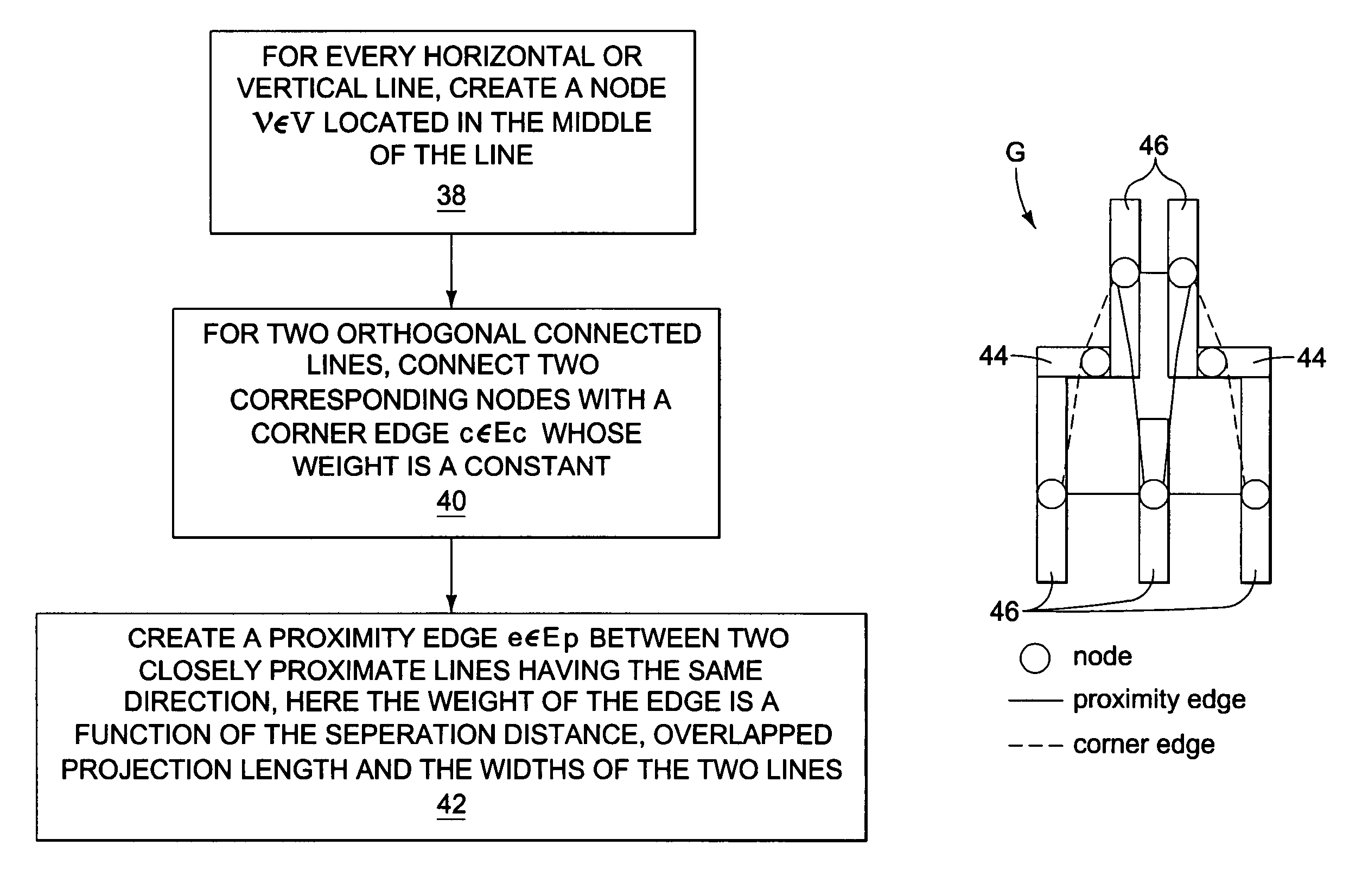
[0018]Briefly, the present invention is directed to a detection method for hotspots induced by lithographic uncertainty. The hotspot detection method includes building a layout graph which reflects pattern-related critical dimension (CD) variation. Given a layout L, the layout graph G=(V, EcâˆȘEp) consists of nodes V, corner edges Ec and proximity edges Ep between the nodes V. A face in the layout graph includes several close features and the edges between them. The weight given to the edges is calculated from a traditional 2-D model. Then a three-level hotspot detection is applied: (1) edge-level detection finds...


PUM


Abstract

Method for detecting hotspots in a circuit layout includes constructing a layout graph having nodes, corner edges and proximity edges from the circuit layout, converting the layout graph to a corresponding dual graph, and iteratively selecting edges and nodes having weights greater than a predetermined threshold value at each iteration as hotspots.

Description

FIELD OF THE INVENTION[0001]The present invention relates to optical lithography, and in particular to a method for detecting hotspots induced by lithographic uncertainties.BACKGROUND OF THE INVENTION[0002]Moore's Law continues to drive higher performance with smaller circuit features. Aggressive technology scaling has introduced new variation sources and made process variation control more difficult. For optical lithography, manufacturability is roughly defined by the k1 factor from the Rayleigh equation. Beyond the 45 nm CMOS technology node, even using a high-end optical exposure system such as immersion lithography with higher numerical aperture (NA), it is necessary to have a k1 factor lower than 0.35. The primary risk posed by lower k1 is the likelihood of degradation of patterning fidelity on VLSI circuits. Lower k1 could decrease patterning fidelity and result in generation of many “hotspots.” A hotspot is an actual device pattern which has relatively large critical dimensio...

Claims


Application Information

Patent Timeline
17 May 2011
Publication
US7945870B2
IPC
G06F17/50
CPC
G06F17/5081; G06F30/398
Inventors
KAHNG, ANDREW B.; PARK, CHUL-HONG