Conductive pattern formation method

a pattern and conductive technology, applied in the direction of printed circuit, sustainable manufacturing/processing, final product manufacturing, etc., can solve the problems of poor connection, limit the processing precision of copper patterns,

Active Publication Date: 2011-05-24
TEXAS INSTR INC
View PDF9 Cites 61 Cited by
  • Summary
  • Abstract
  • Description
  • Claims
  • Application Information

AI Technical Summary

Problems solved by technology

When solder plating is formed with this method, there are the following problems.
Either way, there are limits to the processing precision of the copper pattern.
But when the solder powder adhered on top of the copper pattern of this straight shape is reflowed, variations are generated in the positions at which the solder protrudes and in the height at which the solder protrudes, so that positive bonding of the stud bump electrodes of the semiconductor chip to the solder cannot be performed, which produces poor connections.

Method used


Image

  • Conductive pattern formation method
  • Conductive pattern formation method
  • Conductive pattern formation method

Examples


Embodiment Construction

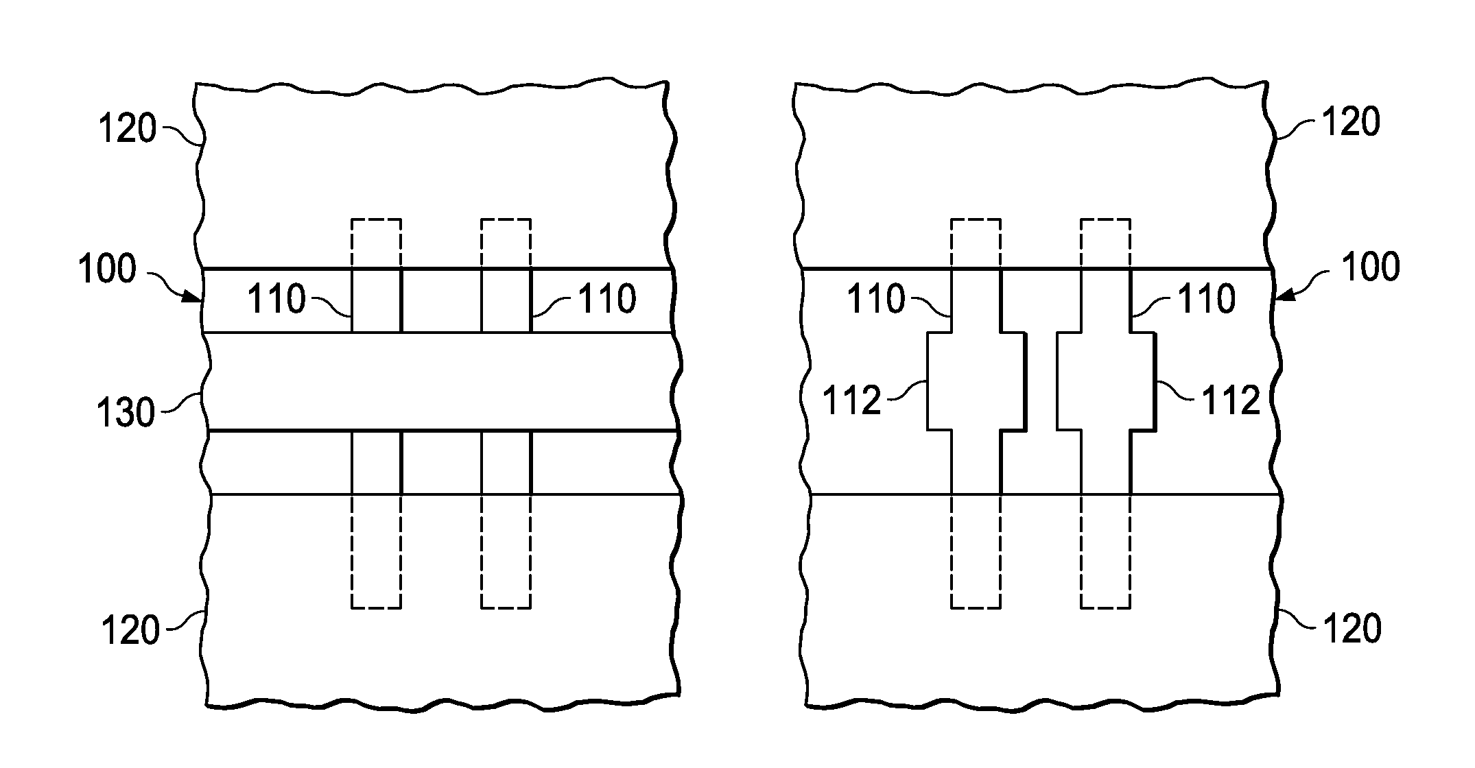
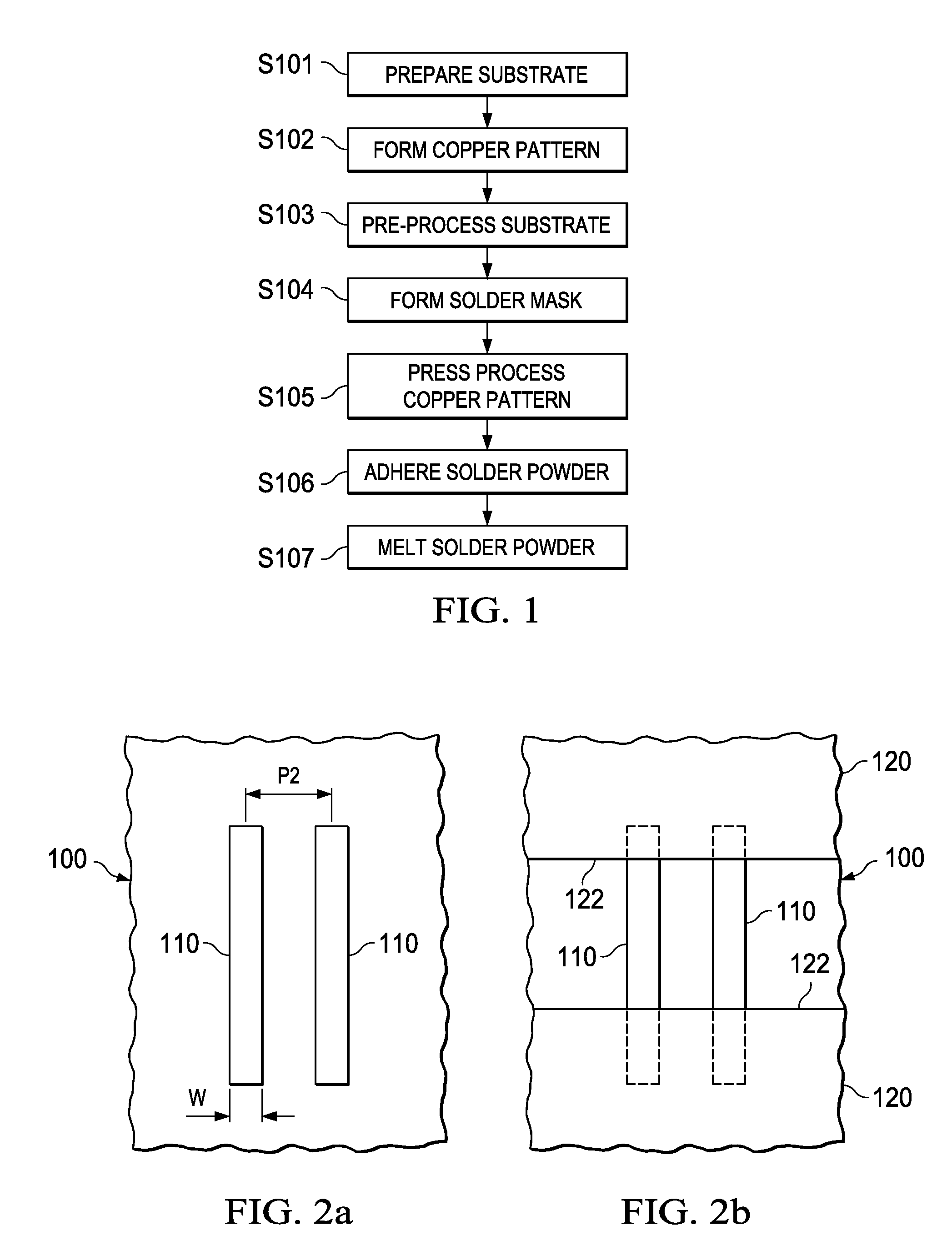
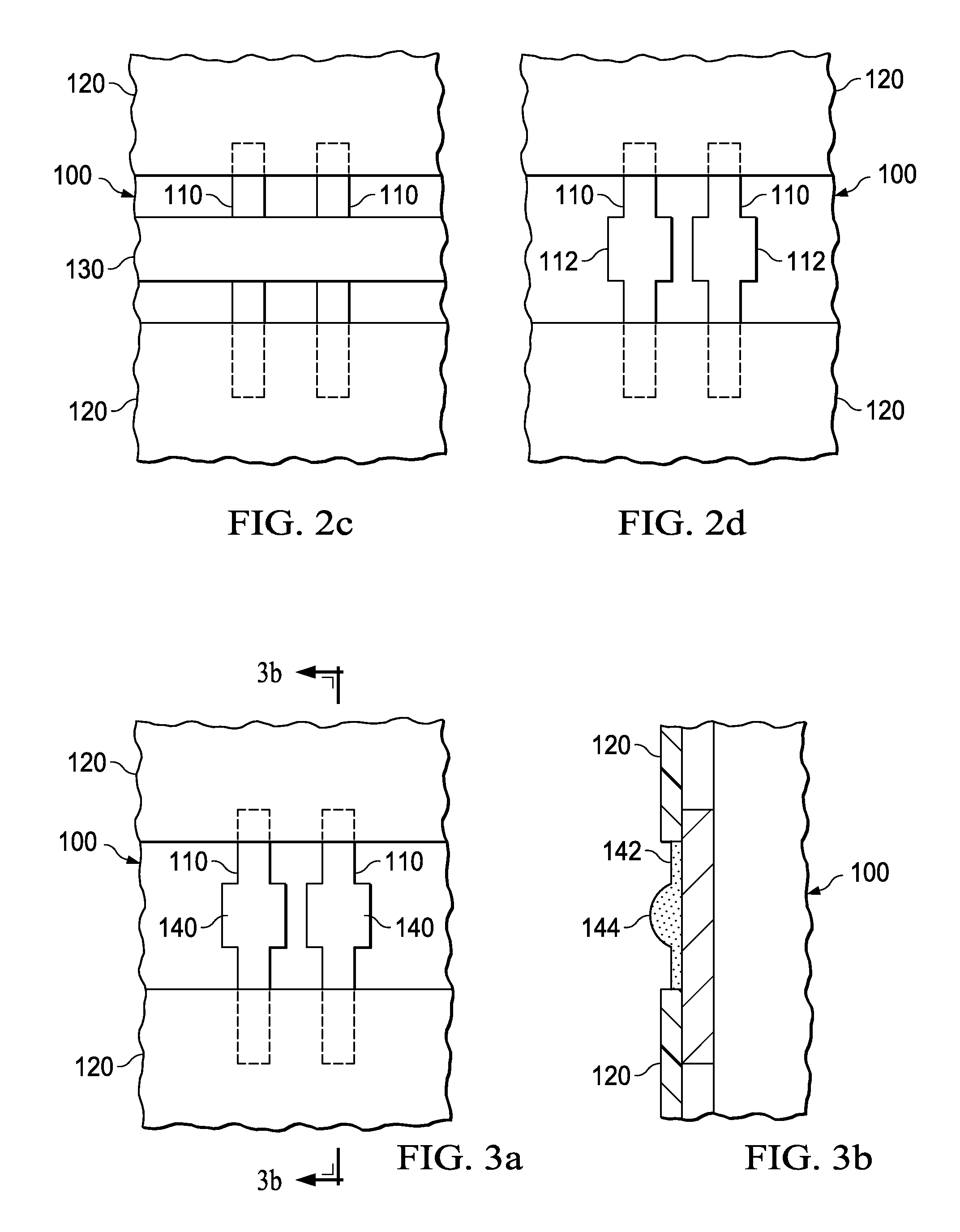
[0024]According to the present invention, the necessity of forming a conductive pattern having wide regions during the formation of the conductive pattern is eliminated, and the formation of a semiconductor pattern with a narrower pitch can be performed. Also, because the wide regions of the conductive pattern are formed by means of pressing the conductive pattern, the process can be simplified. Alternatively, by making the exposed surface area of the conductive pattern larger in the center section than in the edge section of the aperture, the surface area at which the solder powder is adhered becomes large in the center section of the aperture, and by this means, the formation of solder protrusions in a fixed region of each conductive pattern can be achieved.

[0025]Preferred embodiment configurations of the present invention are explained below in detail with reference to the drawing figures. Here, a semiconductor device in which a flip chip is mounted is used in the example.

[0026]F...


PUM

PropertyMeasurementUnit
distanceaaaaaaaaaa
widthaaaaaaaaaa
widthaaaaaaaaaa

Abstract

The objective of the present invention is to offer a method for forming a conductive pattern on a substrate and solder protrusions on the conductive pattern. The pitch of the conductive pattern corresponds to the pitch of electrodes on a semiconductor chip.

Description

FIELD OF THE INVENTION[0001]The present invention relates to a method which forms conductive patterns on top of a substrate, and in particular, relates to a method in which copper patterns that are formed on the substrate used for a flip chip are solder plated.BACKGROUND OF THE INVENTION[0002]Accompanying the popularization of portable telephones, portable computers, and other small electronic devices, the demand for increasingly miniaturized and thinner devices which contain semiconductor elements has increased. In order to answer this demand, the BGA package and the CSP package have been developed and put into practical use. For example, in Japanese Kokai Patent No. Hei 11[1999]-345837, a method for the manufacture of a BGA package is disclosed in which the semiconductor chip is a flip chip or is made to face down, and an underfilling processing is performed between the substrate and the semiconductor chip.[0003]In the case of the flip-chip mounting of a semiconductor chip, on the...

Claims


Application Information

Patent Timeline
Patent Type & Authority Patents(United States)
IPC IPC(8): H01L21/44
CPCH01L21/4853H01L23/49838H05K1/111H05K3/3452H05K3/3484Y10T29/49151H01L24/81H01L2224/05552H01L2224/1148H01L2224/13144H01L2224/16H01L2224/8121H01L2224/81815H01L2924/01078H01L2924/01079H01L2924/15311H05K2201/09727H05K2201/0989H05K2201/10674H05K2203/0278H05K2203/043H01L21/563H01L2224/81193H01L2224/0401H01L2924/00012H01L2224/16237H01L2224/81385H01L2924/14H05K3/3485Y02P70/50H01L2924/00
Inventor ITO, CHIZUKOMASUMOTO, MUTSUMI
Owner TEXAS INSTR INC
Why Eureka
Try Eureka