Sensor having a thin-film inhibition layer

a sensor and inhibition layer technology, applied in the direction of instruments, physical/chemical process catalysts, gas-gas reaction processes, etc., can solve the problems of high cost, weight and complexity, and the conventional no detection strategy suffers limitations in equipment size, weight, cost and/or operational complexity, and achieves rapid and reversible, high sensitivity, and large dynamic range

Active Publication Date: 2011-05-24
NANOMIX INC
View PDF166 Cites 26 Cited by
  • Summary
  • Abstract
  • Description
  • Claims
  • Application Information

AI Technical Summary

Benefits of technology

[0028]Particular embodiments for breath-species analysis and monitoring, and in particular the measurement of endogenous NO as a breath marker, bring the advantages of novel nanostructured electronic sensors to medical applications: (i) performance that matches or exceeds that of infrared technology; (ii) plug-and-play simplicity in a disposable package; (iii) the small size and low power consumption needed for portability and / or wireless integration; (iv) the ability to incorporate arrays of sensors on a single chip; and (v) an order of magnitude reduction in the cost of the sensor component.
[0030]Exemplary embodiments of sensor devices having aspects of the invention provide for detection of chemical, physiologic, or biomolecular species employing nanostructures as elements, both for use in gaseous and in liquid media, such as biological fluids, electrolytes, and the like. Real time electronic detection and monitoring and offers high sensitivity, is rapid and reversible, and has a large dynamic range. The output is digital so electronic filtering and post processing may be used to eliminate extraneous noise, if need be. Certain embodiments include multiplexed assays on a single sensor platform or chip.
[0031]Alternative embodiments having aspects of the invention are configured for detection of analytes employing nanostructured sensor elements configured as one or more alternative types of electronic devices, such as capacitive sensors, resistive sensors, impedance sensors, field effect transistor sensors, electrochemical sensors, and the like, or combinations thereof. Two or more such measurement strategies in a may be included in a sensor device so as to provide orthogonal measurements that increase accuracy and / or sensitivity. Embodiments may have functionalization groups or material associated with nanostructured elements to provide sensitive, selective analyte response.
[0032]Nanotubes were first reported in 1993 by S. Iijima and have been the subject of intense research since. Single walled nanotubes (SWNTs) are characterized by strong covalent bonding, a unique one-dimensional structure, and exceptionally high tensile strength, high resilience, metallic to semiconducting electronic properties, high current carrying capacity, and extreme sensitivity to perturbations caused by charged species in proximity to the nanotube surface.
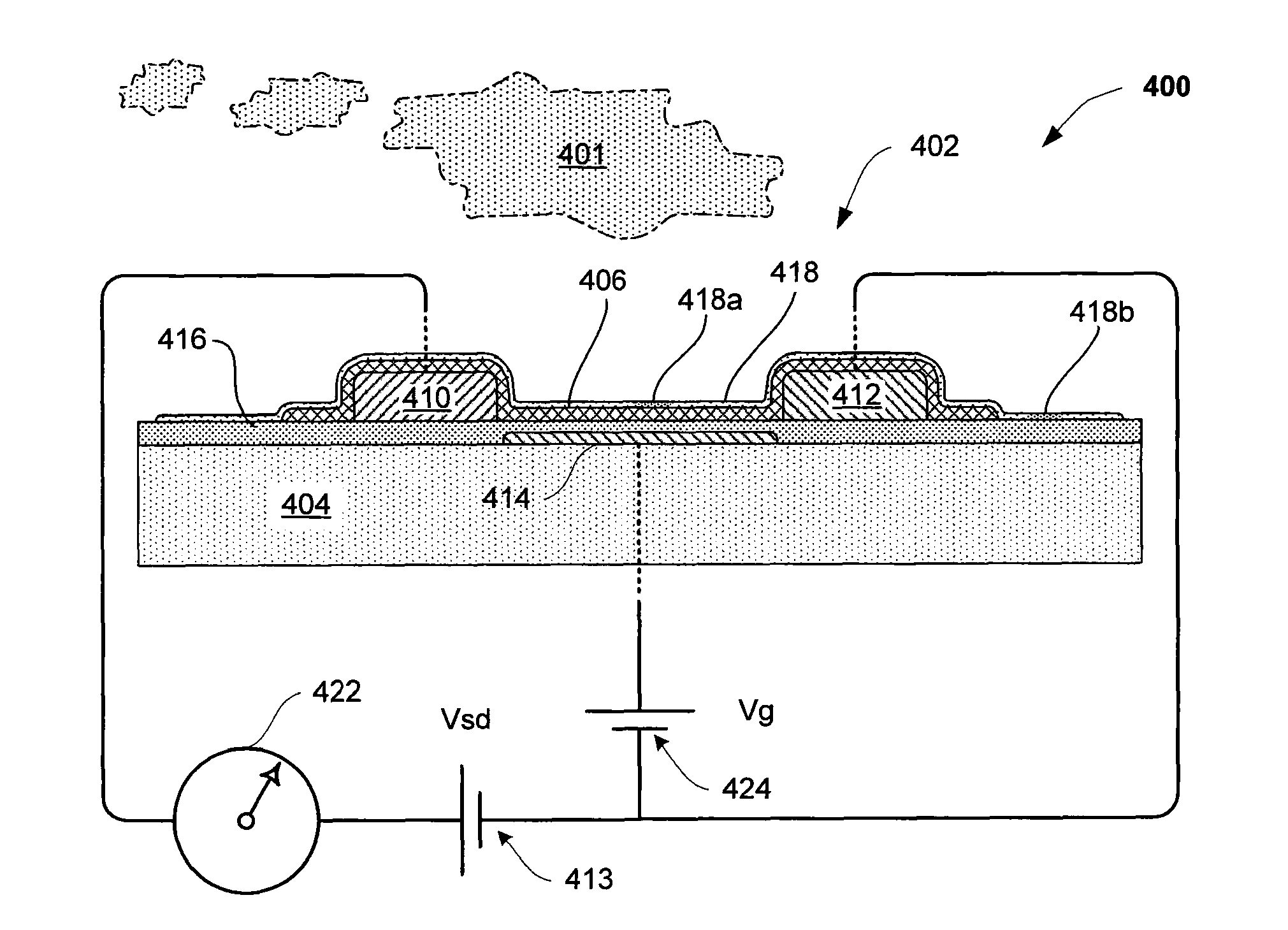
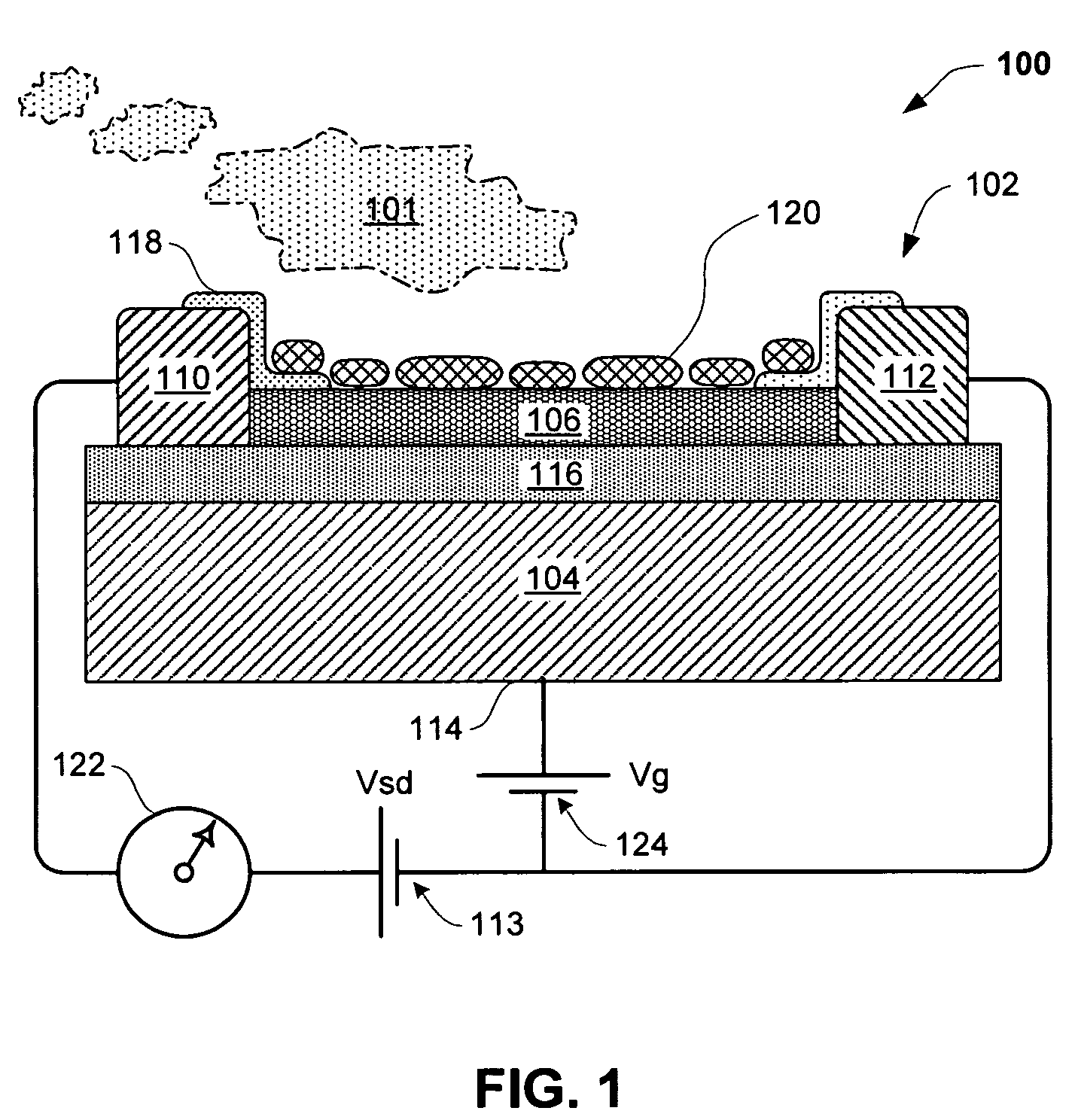
[0046]Sensor with thin film functionalization / inhibition layer. One exemplary embodiment having aspects of the invention of a sensor device for detecting an analyte species in a gas or liquid sample medium, comprises (a) a substrate having a substrate surface; (b) one or more nanostructures disposed over the substrate surface; (c) one or more conducting elements in electrical communication with the nanostructure and configured to communicate with measurement circuitry; and (d) a functionalization / inhibition layer disposed so as to cover all or a portion of the one or more nanostructures; and to cover all or a portion of the substrate surface, the layer configured and composed so as to: (i) permit at least one interaction between the one or more nanostructures and the analyte species; so as to provide a detectable change in a property of the nanostructure in response to the presence of the analyte in the sample; and (ii) inhibit at least one interaction between the substrate surface and the sample medium, so as to prevent or reduce at least one interference response of the device which would be detectable by the measurement circuitry via the one or more conducting elements in the absence of the functionalization layer. The functionalization layer can also provide inhibition for exposed portions of electrical contacts.
[0048]NO to NO2 conversion device. One exemplary embodiment having aspects of the invention of a NO to NO2 conversion device for converting endogenous NO to NO2 in an exhaled breath sample for subsequent measurement of the produced NO2, and comprises (a) an conduit including in communicating sequence: (i) an inlet portion configured to receive the breath sample under an input pressure sufficient to induce flow in the conduit, (ii) a conversion portion, and (iii) an outlet portion configured to dispense the breath sample following conversion; and (b) a conversion material disposed within the conversion portion, the conversion material comprising an active substance promoting conversion of NO to NO2 and a carrier material configured to support the active substance in contact with the breath sample, the conversion material configured to provide minimal pressure drop during sample flow across the conversion portion, to provide high conversion efficiency of NO to NO2, and to provide low loss of NO and / or NO2 via destruction or absorption.

Problems solved by technology

However, medical systems for the measurement of NO suffer from generally the same limitations as capnograph devices, e.g., high cost, weight and complexity.
However, each of the conventional NO detection strategies suffer limitations in equipment size, weight, cost and / or operational complexity that limit their use for a low-cost, patent-portable.

Method used


Image

  • Sensor having a thin-film inhibition layer
  • Sensor having a thin-film inhibition layer
  • Sensor having a thin-film inhibition layer

Examples


Embodiment Construction

1. Nanosensor Architecture.

[0071]FIG. 1. shows an exemplary electronic sensing device 100 having aspects of the invention, for detecting an analyte 101, such as biomolecule, organic and inorganic species, including environmentally and medically relevant volatiles and gases, such as NO, NO2, CO2, NH3, H2, H2O2, CO and the like. Sensing device 100 comprises a nanostructure sensor 102. Sensor 102 comprises a substrate 104, and a conducting channel or layer 106 comprising a nanostructure material, such as a nanotube or network of nanotubes, disposed on the substrate. The nanostructure material 106 may contact the substrate as shown, or in the alternative, may be spaced a distance away from the substrate, with or without a layer of intervening material.

[0072]In an embodiment of the invention, conducting channel 106 may comprise one or more carbon nanotubes. For example, conducting channel 106 may comprise a plurality of nanotubes forming a mesh, film or network. Certain exemplary embodim...


PUM

PropertyMeasurementUnit
thicknessaaaaaaaaaa
thicknessaaaaaaaaaa
thicknessaaaaaaaaaa

Abstract

Sensors and detection systems suitable for measuring analytes, such as biomolecule, organic and inorganic species, including environmentally and medically relevant volatiles and gases, such as NO, NO2, CO2, NH3, H2, CO and the like, are provided. Certain embodiments of nanostructured sensor systems are configured for measurement of medically important gases in breath. Applications include the measurement of endogenous nitric oxide (NO) in breath, such as for the monitoring or diagnosis of asthma and other pulmonary conditions.

Description

CROSS-REFERENCE TO RELATED APPLICATIONS[0001]This application claims the benefit pursuant to 35 USC. 119(e) of the following US Provisional Applications, each of which applications are incorporated by reference:[0002]U.S. Application No. 60 / 967,552 filed Sep. 4, 2007, entitled “Sensor Having A Thin-Film Inhibition Layer, Nitric Oxide Converter And Monitor”; and[0003]U.S. Application No. 60 / 922,642 filed Apr. 10, 2007, entitled “Ammonia Nanosensors, and Environmental Control System”;[0004]This application claims priority pursuant to 35 USC. §120 of the following U.S. Applications, each of which applications are incorporated by reference:[0005]U.S. Ser. No. 11 / 636,360 filed Dec. 8, 2006 (published 2008-0093226), entitled “Ammonia Nanosensors, and Environmental Control System”; which claims priority to US provisional application. No. 60 / 748,834 filed Dec. 9, 2005;[0006]U.S. Ser. No. 11 / 588,845 filed Oct. 26, 2006 (published 2008-0021339), entitled “Anesthesia Monitor, Capacitance Nanos...

Claims


Application Information

Patent Timeline
Patent Type & Authority Patents(United States)
IPC IPC(8): H01L27/14
CPCG01N27/127G01N27/4146G01N33/004B82Y30/00G01N33/0037G01N33/497Y02A50/20
Inventor BRYANT, CRAIGCHANG, YING-LANGABRIEL, JEAN-CHRISTOPHE P.JOHNSON, BRADLEY N.KUZMYCH, OLEKSANDRMICKELSON, WILLIAMPASSMORE, JOHN LORENSKARUPO, SERGEIVALCKE, CHRISTIAN
Owner NANOMIX INC
Why Eureka
Try Eureka