Semiconductor memory device and data error detection and correction method of the same

a technology of memory device and semiconductor chip, which is applied in the direction of digital storage, instruments, coding, etc., can solve the problems of increasing chip size, and reducing the yield of semiconductor chip

Inactive Publication Date: 2011-05-24
SAMSUNG ELECTRONICS CO LTD
View PDF21 Cites 11 Cited by
  • Summary
  • Abstract
  • Description
  • Claims
  • Application Information

AI Technical Summary

Problems solved by technology

However, due to the high performance of a semiconductor integrated circuit, when the size of the semiconductor chip increases, the yield of the semiconductor chip decreases in proportion to the increase in size.
Moreover, increasing the degree of integration further decreases the yield of the semiconductor chip.
Applying an ECC to a non-volatile memory device may cause an increase in chip size due to the addition of a parity cell or a speed delay on the error correction circuit.
However, such applications may enhance reliability and yield.
In a conventional semiconductor memory device, where an ECC memory cell is separately disposed in each memory bank, the effect of data error detection and correction may be significant.
However, an overhead problem may be caused due to the addition in error detection and correction of all data.
A defect relief circuit such as a redundant data error detection and correction circuit can be employed to improve the SER, however, the overhead is significantly increased due to the addition of error detection and correction circuits for all the data in a conventional semiconductor memory device having a conventional memory bank structure.

Method used


Image

  • Semiconductor memory device and data error detection and correction method of the same
  • Semiconductor memory device and data error detection and correction method of the same
  • Semiconductor memory device and data error detection and correction method of the same

Examples


Embodiment Construction

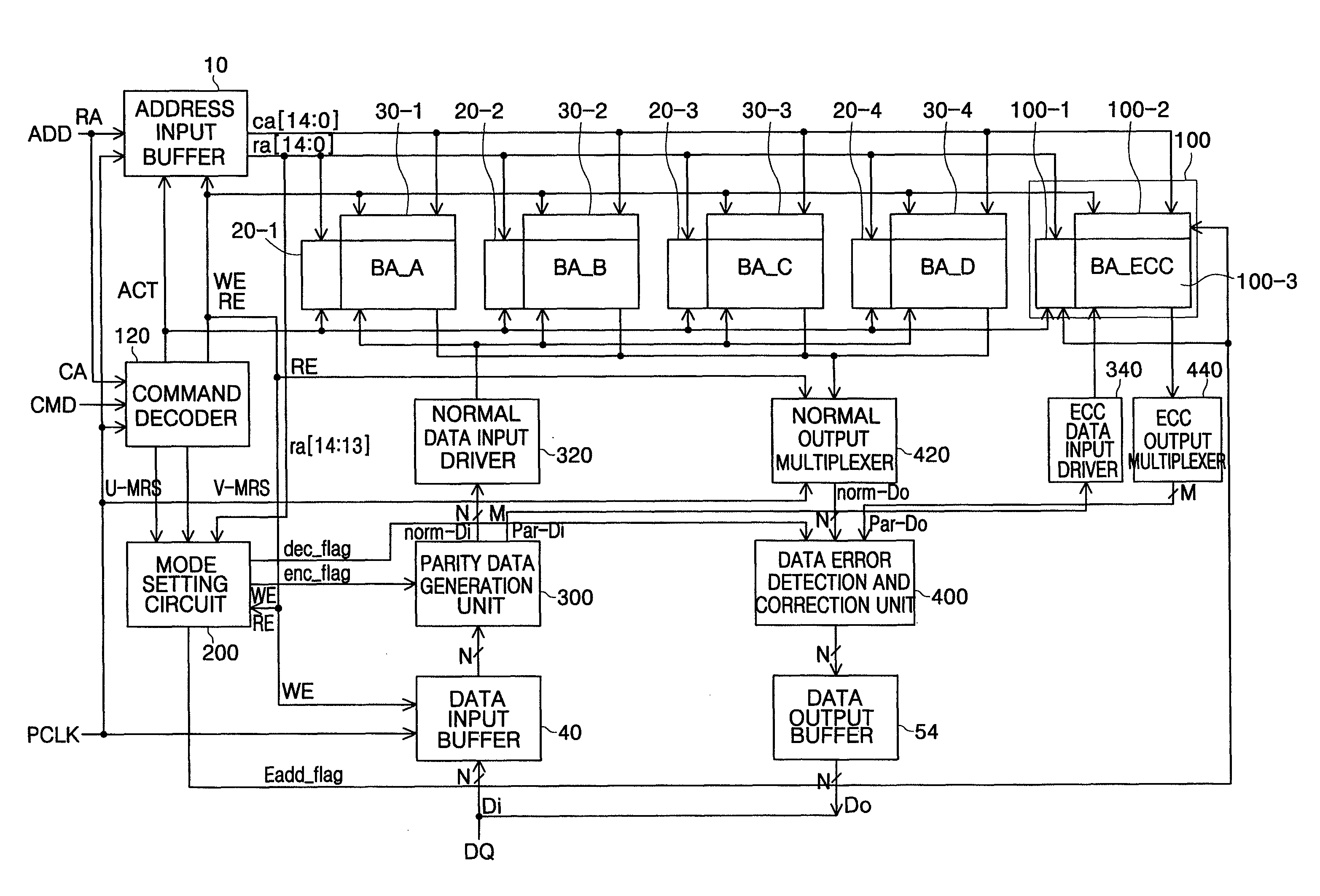
[0066]Hereinafter, exemplary embodiments of the present invention will be described in detail with reference to the accompanying drawings. This invention may, however, be embodied in different forms and should not be construed as limited to the embodiments set forth herein.

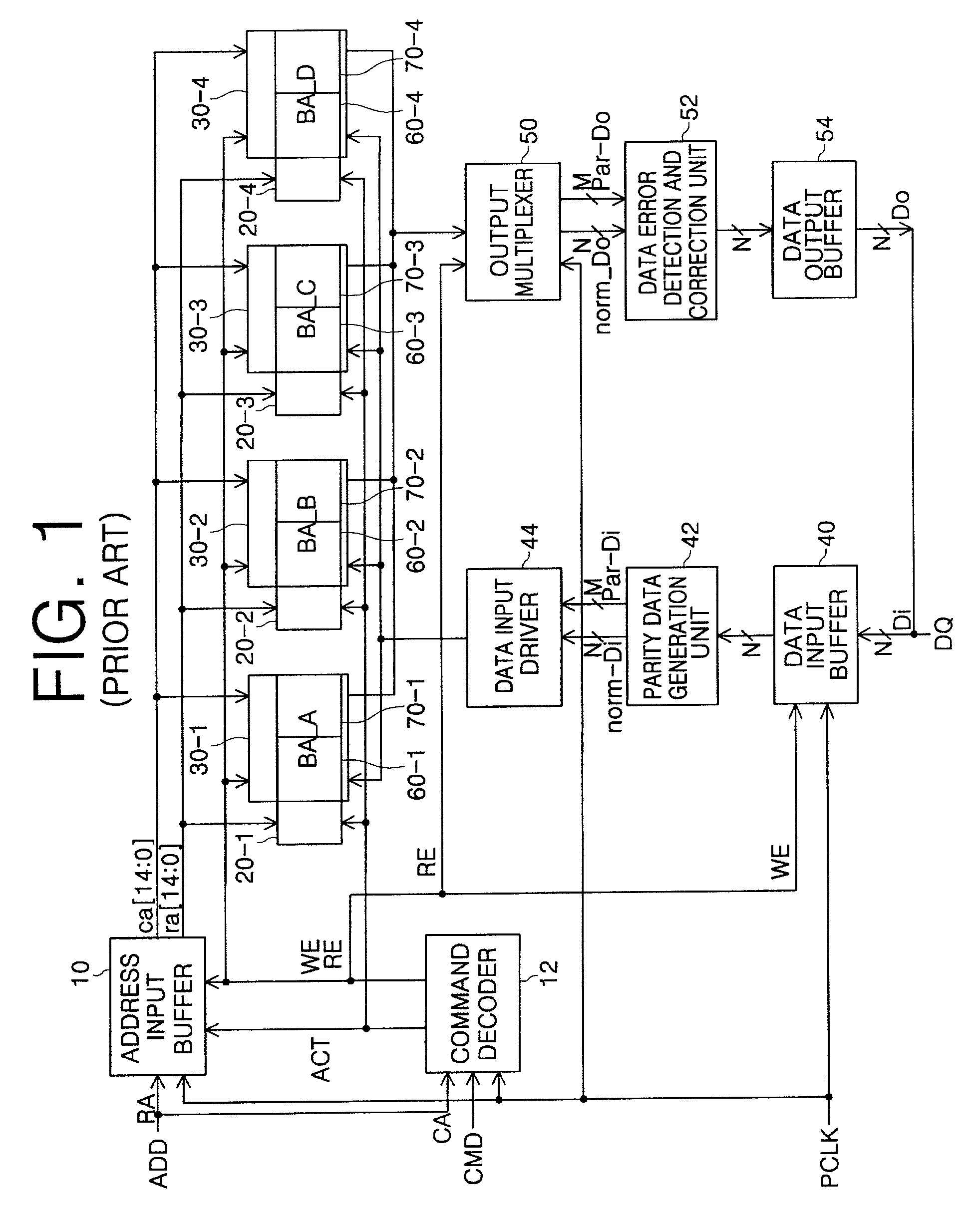
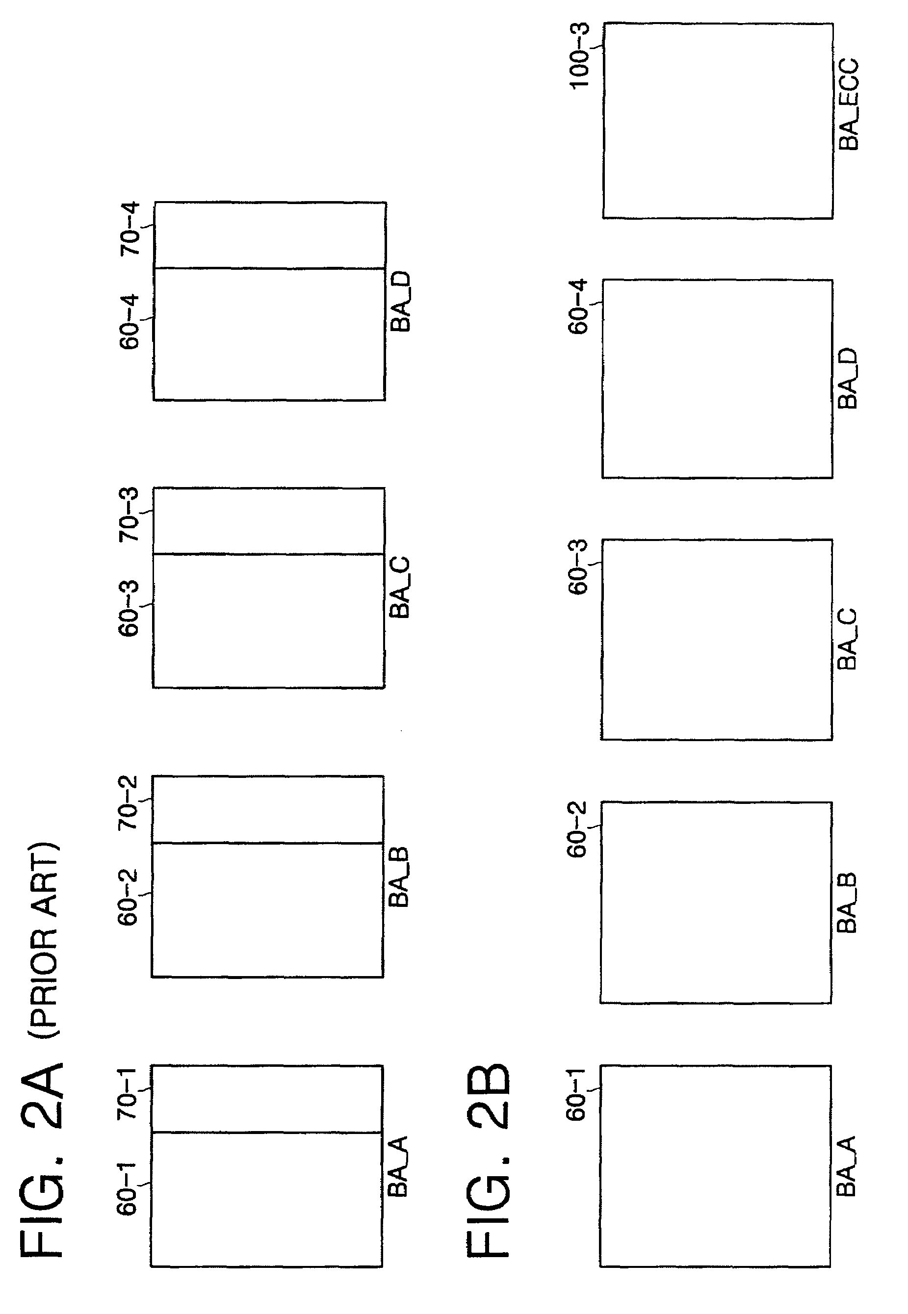
[0067]FIG. 2A is a configuration diagram of a memory cell array within a conventional semiconductor memory device, and FIG. 2B is a configuration diagram of a memory cell array within a semiconductor memory device in accordance with an exemplary embodiment of the present invention.

[0068]Referring to FIG. 2A, the memory cell array within the conventional semiconductor memory device includes a plurality of memory banks BA_A, BA_B, BA_C and BA_D which include respective normal memory cells 60-1, 60-2, 60-3 and 60-4 and respective ECC memory cells 70-1, 70-2, 70-3 and 70-4. For ease of discussion, it is assumed that the memory cell array includes four memory banks.

[0069]Each of the memory banks BA_A, BA_B, BA_C and BA...


PUM


Abstract

A semiconductor memory device includes a memory cell array, a mode setting circuit, a parity data generation unit, and a data error detection and correction unit. The memory cell array has a plurality of first memory banks for storing normal data, and a predetermined number of second memory banks less than the number of the first memory banks for storing parity data according to control of a first flag signal. The mode setting circuit sets the first flag signal and a second flag signal controlling based on whether a separate memory bank is used to store the parity data in the second memory banks. The parity data generation unit receives normal write data during a write operation, generates parity data with respect to the normal write data in response to the second flag signal, and outputs the normal data and the parity data. The data error detection and correction unit receives normal read data and parity read data read from the memory cell array during a read operation, detects errors of the normal read data in response to the second flag signal, corrects the normal read data when the errors are detected, and outputs the corrected read data.

Description

CROSS-REFERENCE TO RELATED APPLICATION[0001]This application claims priority to Korean Patent Application No. 2006-108422, filed on Nov. 3, 2006, the disclosure of which is incorporated by reference in its entirety herein.BACKGROUND OF THE INVENTION[0002]1. Technical Field[0003]The present disclosure relates to a semiconductor memory device, and more particularly, to a semiconductor memory device which allocates memory banks having memory cells storing data for detecting data errors, correcting data errors, and enhancing the yield of a semiconductor chip.[0004]2. Discussion of the Related Art[0005]Rapid progress in semiconductor technology development has resulted in high integration and high performance semiconductor integrated circuits, and in particular, remarkably high integration has been attained in the field of semiconductor memory devices.[0006]However, due to the high performance of a semiconductor integrated circuit, when the size of the semiconductor chip increases, the y...

Claims


Application Information

Patent Timeline
Patent Type & Authority Patents(United States)
IPC IPC(8): G11C29/00
CPCG06F11/1008G11C8/12G11C8/04G06F11/1076G11C29/00
Inventor LEE, KWANG-JINLEE, WON-SEOKKIM, DU-EUNG
Owner SAMSUNG ELECTRONICS CO LTD
Why Eureka
Try Eureka