Water-barrier encapsulation method

a technology of light-emitting diodes and water-barriers, which is applied in the direction of electric lighting sources, solid-state devices, and light-emitting devices. it can solve the problems of increasing drive voltage, reducing electroluminescence efficiency, and limited life of display devices, so as to reduce oxygen penetration, and increase the lifetime of the oled structure

Active Publication Date: 2011-05-31
APPLIED MATERIALS INC
View PDF9 Cites 16 Cited by
  • Summary
  • Abstract
  • Description
  • Claims
  • Application Information

AI Technical Summary

Benefits of technology

[0008]The present invention generally relates to OLED structures and methods for their manufacture. To increase the lifetime of an OLED structure, an encapsulating layer may be deposited over the OLED structure. The encapsulating layer may fully enclose or “encapsulate” the OLED structure. The encapsulating layer may have a substantially planar surface opposite to the interface between the OLED structure and the encapsulating layer. The planar surface permits successive layers to be evenly deposited over the OLED structure. The encapsulating layer reduces any oxygen penetration into the OLED structure and may increase the lifetime of the OLED structure.

Problems solved by technology

The lifetime of display devices can be limited, characterized by a decrease in electroluminescence efficiency and an increase in drive voltage.
The limited lifetime may be due to the degradation of organic or polymer materials and the formation of non-emissive dark spots.
Material degradation and dark spot problems may be caused by moisture and oxygen ingress.
In addition, exposure to air or oxygen may cause cathode oxidation.

Method used


Image

  • Water-barrier encapsulation method
  • Water-barrier encapsulation method
  • Water-barrier encapsulation method

Examples


Embodiment Construction

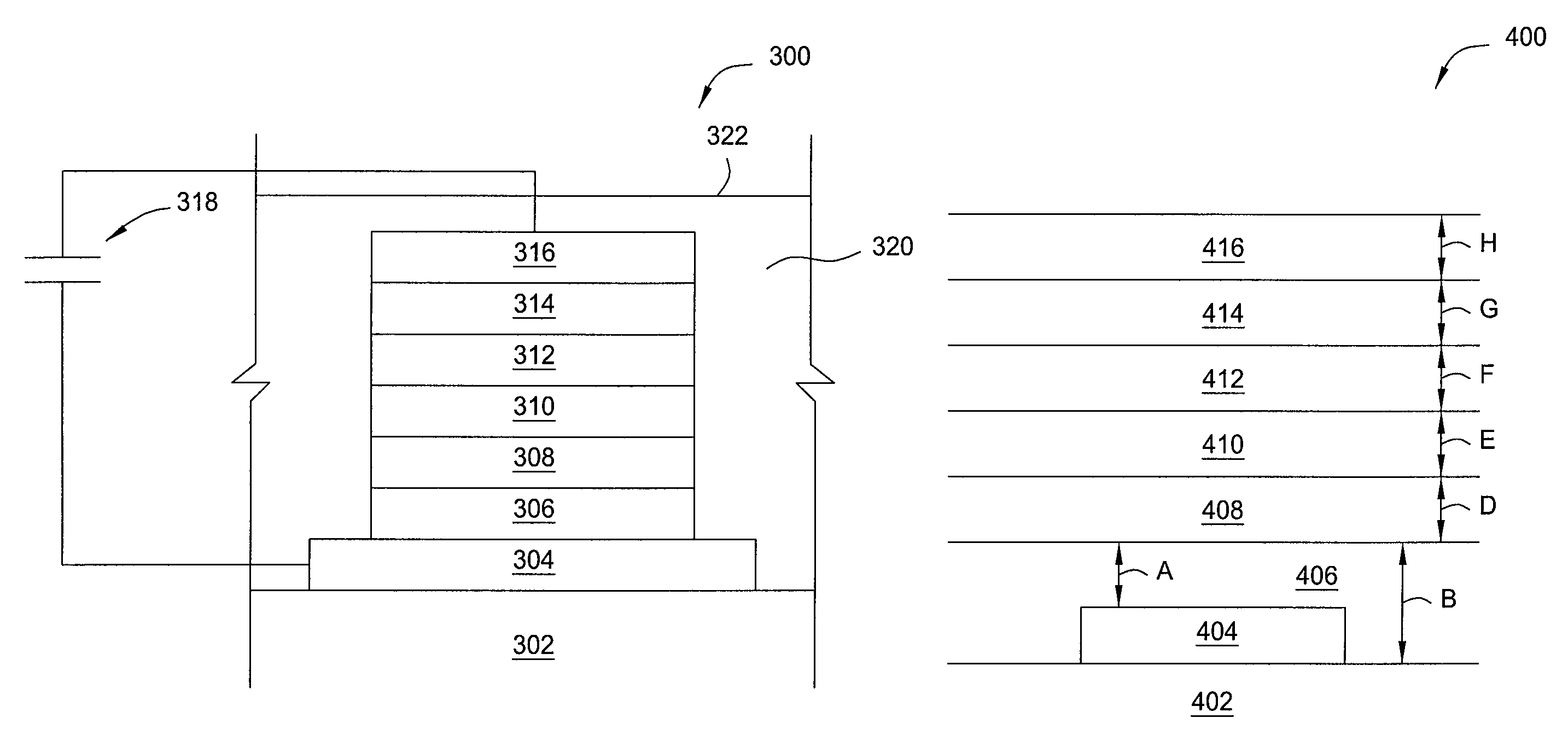
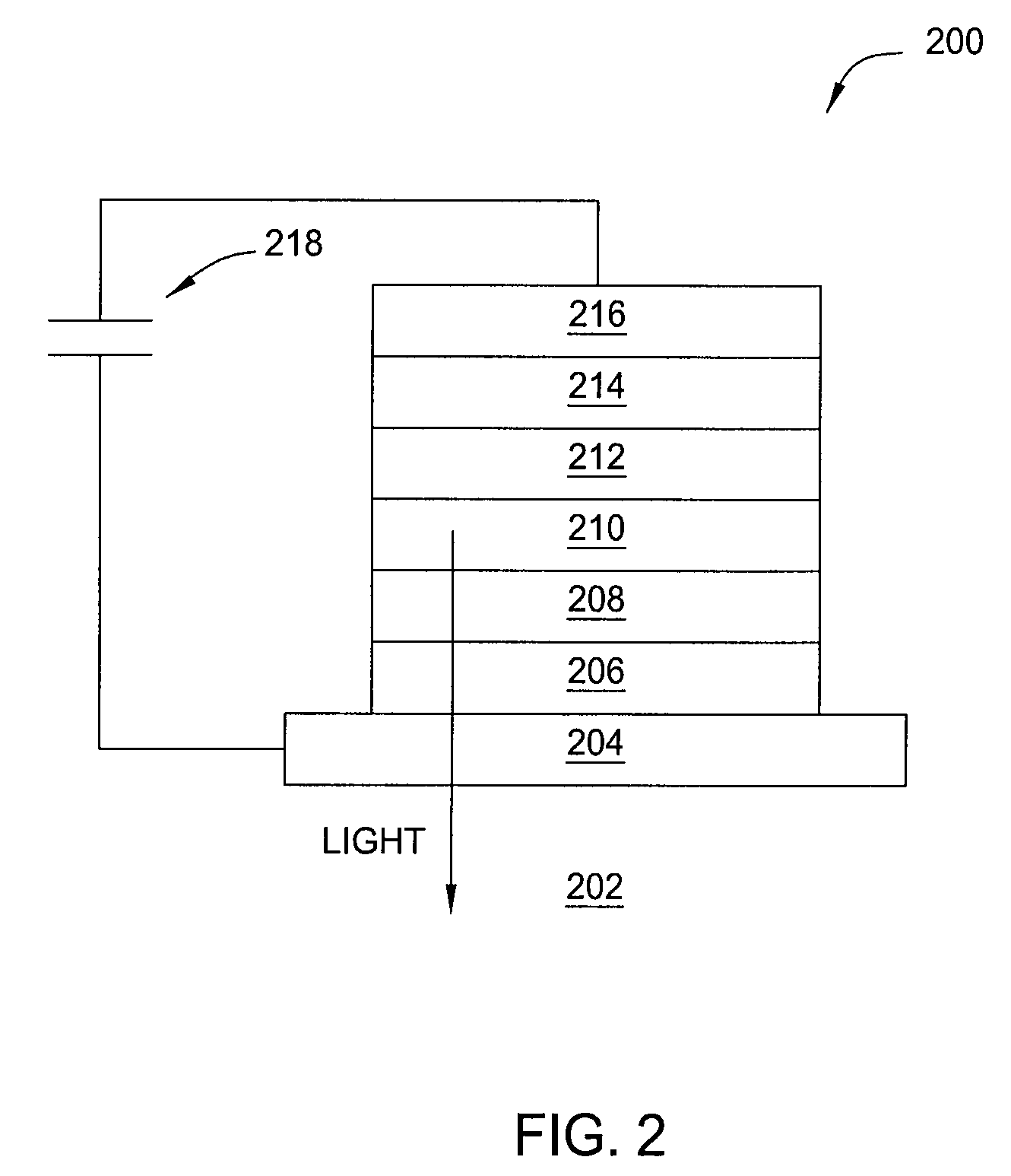
[0018]The present invention generally relates to OLED structures and methods for their manufacture. To increase the lifetime of an OLED structure, an encapsulating layer may be deposited over the OLED structure. The encapsulating layer may fully enclose or “encapsulate” the OLED structure. The encapsulating layer may have a substantially planar surface opposite to the interface between the OLED structure and the encapsulating layer. The planar surface permits successive layers to be evenly deposited over the OLED structure. The encapsulating layer reduces any oxygen penetration into the OLED structure and may increase the lifetime of the OLED structure.

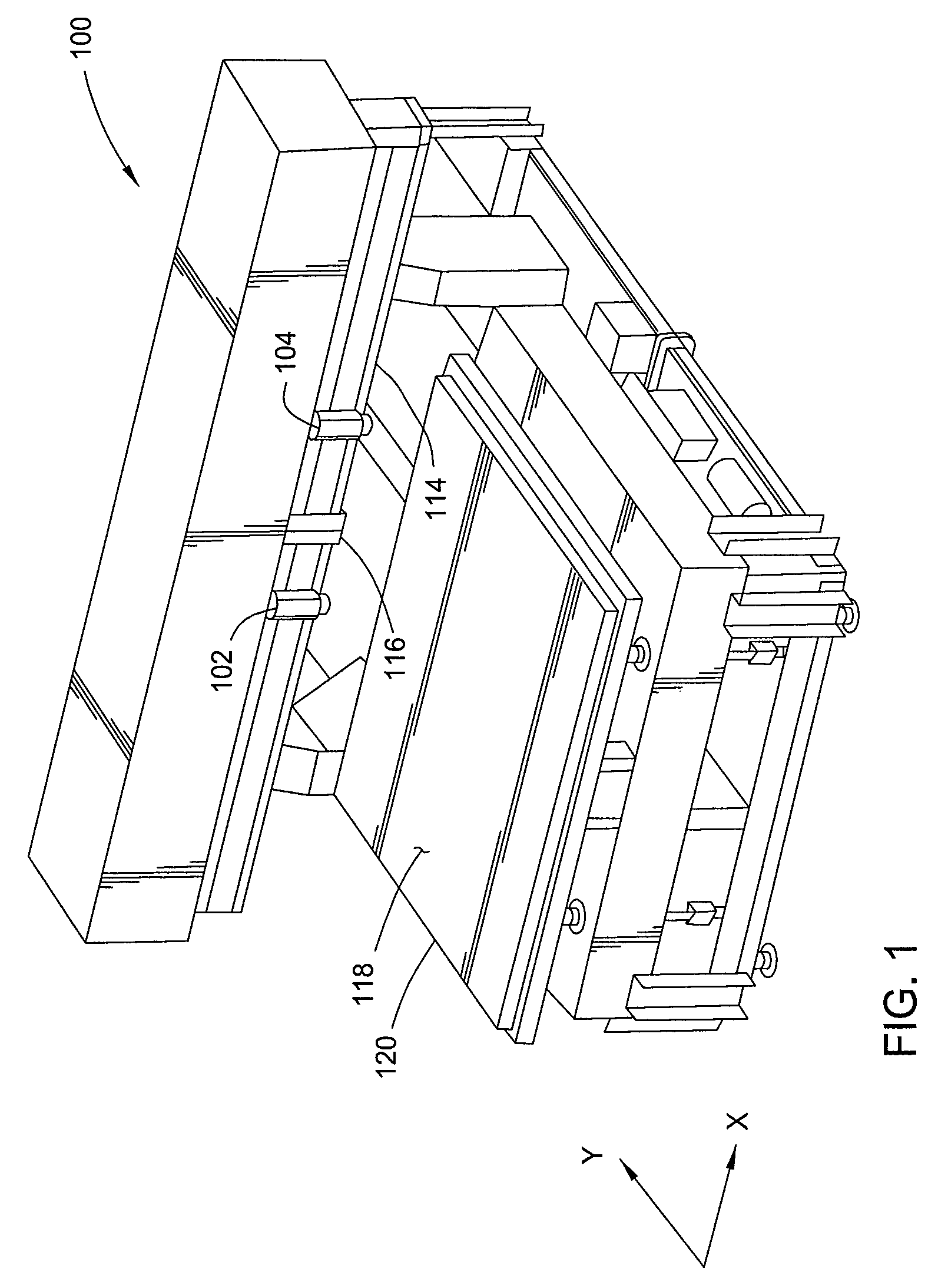
[0019]FIG. 1 is a schematic perspective view of an apparatus 100 for inkjet printing according to one embodiment of the invention. It is to be understood that while two inkjet heads 102, 104, have been shown, more or less inkjet heads may be present. The apparatus 100 also includes a bridge 114 on which the inkjet heads 102, 104, are ...


PUM


Abstract

The present invention generally relates to organic light emitting diode (OLED) structures and methods for their manufacture. To increase the lifetime of an OLED structure, an encapsulating layer may be deposited over the OLED structure. The encapsulating layer may fully enclose or “encapsulate” the OLED structure. The encapsulating layer may have a substantially planar surface opposite to the interface between the OLED structure and the encapsulating layer. The planar surface permits successive layers to be evenly deposited over the OLED structure. The encapsulating layer reduces any oxygen penetration into the OLED structure and may increase the lifetime of the OLED structure.

Description

CROSS-REFERENCE TO RELATED APPLICATIONS[0001]This application claims benefit of U.S. Provisional Patent Application Ser. No. 61 / 036,230 (APPM / 012814L), filed Mar. 13, 2008, which is herein incorporated by reference.BACKGROUND OF THE INVENTION[0002]1. Field of the Invention[0003]Embodiments of the present invention generally relate to an organic light emitting diode (OLED) structure and a method for its manufacture.[0004]2. Description of the Related Art[0005]OLED displays have gained significant interest recently in display applications in view of their faster response times, larger viewing angles, higher contrast, lighter weight, lower power, and amenability to flexible substrates, as compared to liquid crystal displays (LCD). In addition to organic materials used in OLEDs, many polymer materials are also developed for small molecule, flexible organic light emitting diode (FOLED) and polymer light emitting diode (PLED) displays. Many of these organic and polymer materials are flexi...

Claims


Application Information

Patent Timeline
Patent Type & Authority Patents(United States)
IPC IPC(8): H01L21/00H01L33/00
CPCH01L51/5237H01L21/6715H10K50/84H10K50/8445H05B33/04H05B33/10H10K50/15H10K50/16H10K50/805H10K50/8426H10K71/00
Inventor WON, TAE K.CAMPO, JOSE MANUEL DIEGUEZYADAV, SANJAY D.
Owner APPLIED MATERIALS INC
Why Eureka
Try Eureka