Solid-state imaging device, driving method thereof, and camera

a technology of solid-state imaging and driving method, which is applied in the direction of code conversion, instruments, television systems, etc., can solve the problems of reducing the accuracy of ad conversion, reducing and not being able to remove, so as to achieve the effect of increasing the delay of carry propagation

Active Publication Date: 2011-05-31
PANASONIC SEMICON SOLUTIONS CO LTD
View PDF31 Cites 30 Cited by
  • Summary
  • Abstract
  • Description
  • Claims
  • Application Information

AI Technical Summary

Benefits of technology

[0047]However, according to the conventional technology for recovering the inverted count values, two stages of selectors are included in the carry propagation path between each flop-flop, which increases delay in carry propagation.
[0048]To put it differently, increased carry propagation delay limits the AD conversion frequency, and prevents acceleration (reducing the clock frequency). The column AD conversion units are usually included as many as the number of columns of pixel array, which is as many as a few thousands columns. Since the delay varies with columns, the column with the longest carry delay limits the AD conversion frequency.
[0053]It is an object of the present invention to provide a solid-state imaging device capable of enhancing the accuracy of AD conversion and including an asynchronous counter capable of switching between up-counting and down-counting actively without limiting the AD conversion frequency, a driving method thereof and a camera.
[0056]Here, the first switching unit may include a plurality of first selectors each of which corresponds to one of the plurality of stages of flip-flops, and each of the plurality of first selectors selects one of two signals respectively outputted from the non-inverted output terminal and the inverted terminal of the corresponding flip-flop, outputs the selected signal to a data input terminal of the corresponding flip-flop and the operation mode is set to the holding mode when the signal outputted from the non-inverted output terminal is selected. With this configuration, since a plurality of first selectors are set outside the carry propagation path, it does not increase the delay in carry propagation. Thus, it is suitable for accelerating the AD conversion frequency.
[0057]Here, the second switching unit may include a plurality of second selectors each of which corresponds to an interval between the plurality of stages of flip-flops, each of the plurality of second selectors selects one of two signals respectively outputted from the non-inverted output terminal and the inverted output terminal of the flip-flop in the previous stage, outputs the selected signal to the clock input terminal of a flip-flop in a subsequent stage, and switches the selection during a period within the holding mode. With this configuration, only one of the second selectors is arranged in each interval between the flip-flops in the carry propagation path, it is possible to avoid the limitation of the AD conversion frequency by the carry propagation delay.
[0060]The present invention enables enhancing accuracy of AD conversion, and active switching of up-counting and down-counting in the asynchronous counter without limiting the AD conversion frequency.FURTHER INFORMATION ABOUT TECHNICAL BACKGROUND TO THIS APPLICATION

Problems solved by technology

However, according to the conventional technology for recovering the inverted count values, two stages of selectors are included in the carry propagation path between each flop-flop, which increases delay in carry propagation.
For example, it causes a problem in the following case.
With the noise component due to the change in digital signal generated by the inversion of bit and another inversion of bit, there is a possibility that the offset component that cannot be removed by the comparator in the previous stage of the column AD conversion unit or an upstream circuit is supplied and reduces the accuracy of the AD conversion.
Thus it is not possible to remove as an offset common to all of the pixels, and there is a possibility that the influence on image quality may be larger.

Method used


Image

  • Solid-state imaging device, driving method thereof, and camera
  • Solid-state imaging device, driving method thereof, and camera
  • Solid-state imaging device, driving method thereof, and camera

Examples


first embodiment

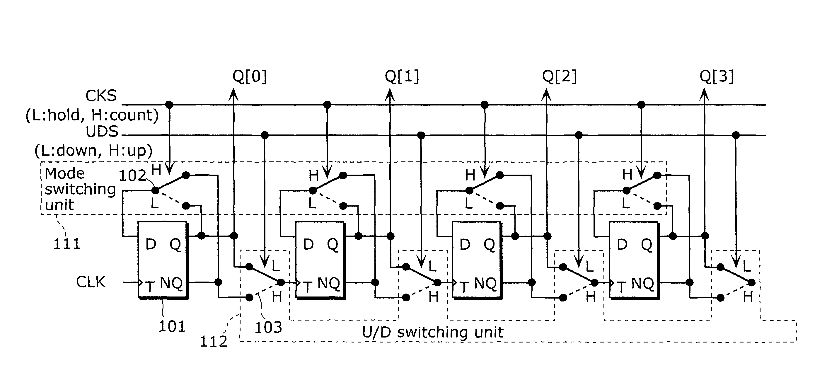
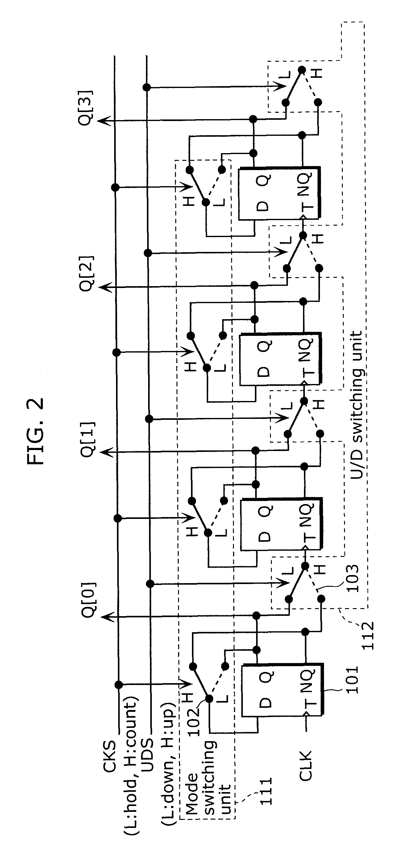
[0075]The feature of the solid-state imaging device according to the present invention is the following three operational modes are included in the column AD conversion unit. More specifically, the asynchronous counter includes an up-counting mode for up-counting, a down-counting mode for down-counting, and a data holding mode in which an operation setting indicating the up-counting and the down-counting is switched while maintaining the count value held in the asynchronous counter.

[0076]With this, switching between the operation setting indicating up-counting and down-counting does not change the count value held in the asynchronous counter, which suppresses generation of noise, and the accuracy of the AD conversion is enhanced. In addition, it is suitable for improving frequency since it does not require a bit inversion and another bit inversion for recovery that were unavoidable in the conventional technology when switching the operation setting.

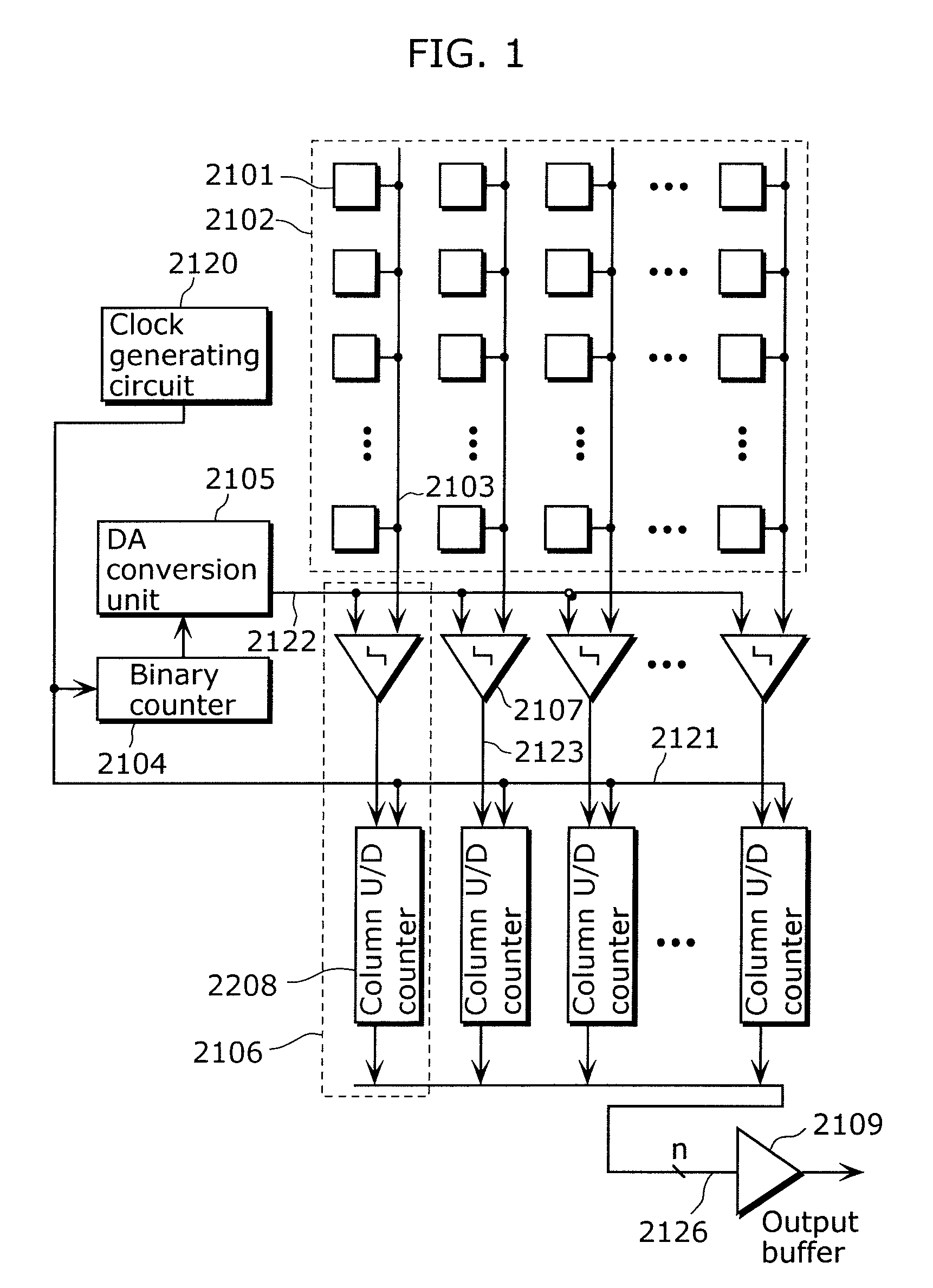
[0077]FIG. 1 is a block diagram sh...

second embodiment

[0113]An asynchronous counter using positive-edge D-FF is described in the first embodiment. An asynchronous counter using negative edge D-FFs is described in the second embodiment.

[0114]The configuration of the solid-state imaging device according to the second embodiment is the same as FIG. 1, and thus the description is omitted except the difference.

[0115]FIG. 4 is a circuit block diagram showing the configuration of the asynchronous counter as the column U / D counter in the second embodiment. A circuit of one-bit in the asynchronous counter is configured through connecting the three circuit components, namely, the D flip-flop 301 with a negative edge reset, the first selector 302, and the second selector 303.

[0116]The connection is, in detail, in the same manner as the output Q and inverted output NQ is connected to input both the first selector 302 and the second selector 303. While the output of the first selector 302 is connected to the data input D of the same flip-flop 301, ...


PUM


Abstract

It is an object of the present invention to provide a solid-state imaging device for enhancing accuracy of AD conversion and active switching of up-counting and down-counting in the asynchronous counter without limiting the AD conversion frequency. The solid-state imaging device according to the present invention includes an asynchronous counter having an up-counting mode in which up-counting is performed, a down-counting mode in which down-counting is performed, and a holding mode for switching operation settings between the up-counting and the down-counting while maintaining a count value held in the asynchronous counter.

Description

BACKGROUND OF THE INVENTION[0001](1) Field of the Invention[0002]The present invention relates to solid-state imaging devices for detecting physical quantity distribution of visible light, electromagnetic waves, and particle radiation such as alpha rays and beta rays, and more particularly to a solid-state imaging device having an asynchronous counter which realizes a CDS operation of AD conversion circuit which receives output signals from the photoelectric conversion device arranged in rows and columns, the driving method thereof, and a camera.[0003](2) Description of the Related Art[0004]In recent years, MOS image sensors (hereinafter referred to as “MOS sensors”) in which peripheral circuits such as an AD conversion circuit can be incorporated have been actively developed, and the number of products has been increasing, as a counterpart of Charge Coupled Devices image sensors (hereinafter referred to as “CCD sensor”), which have established their use as image sensors, that is, t...

Claims


Application Information

Patent Timeline
Patent Type & Authority Patents(United States)
IPC IPC(8): H03M1/34H03M1/56H04N5/335H04N5/357H04N5/363H04N5/374H04N5/376H04N5/378
CPCH03M1/1023H03M1/1295H03M1/125H03M1/123H03M1/56
Inventor SHIMOMURA, KENICHIWATANABE, KENJI
Owner PANASONIC SEMICON SOLUTIONS CO LTD
Why Eureka
Try Eureka