Optical member with retardation control function and liquid crystal display
a technology of optical member and retardation layer, which is applied in the direction of optics, instruments, optical elements, etc., can solve the problems of deformation of liquid crystal cell gap by 15% or more, the inability to secure a definite cell gap, and the inability to maintain the cell gap so as to achieve the effect of inhibiting the retardation layer from subsiding, improving the productivity of liquid crystal cell, and high quality
- Summary
- Abstract
- Description
- Claims
- Application Information
AI Technical Summary
Benefits of technology
Problems solved by technology
Method used
Image
Examples
example 1
Formation of Colored Layer
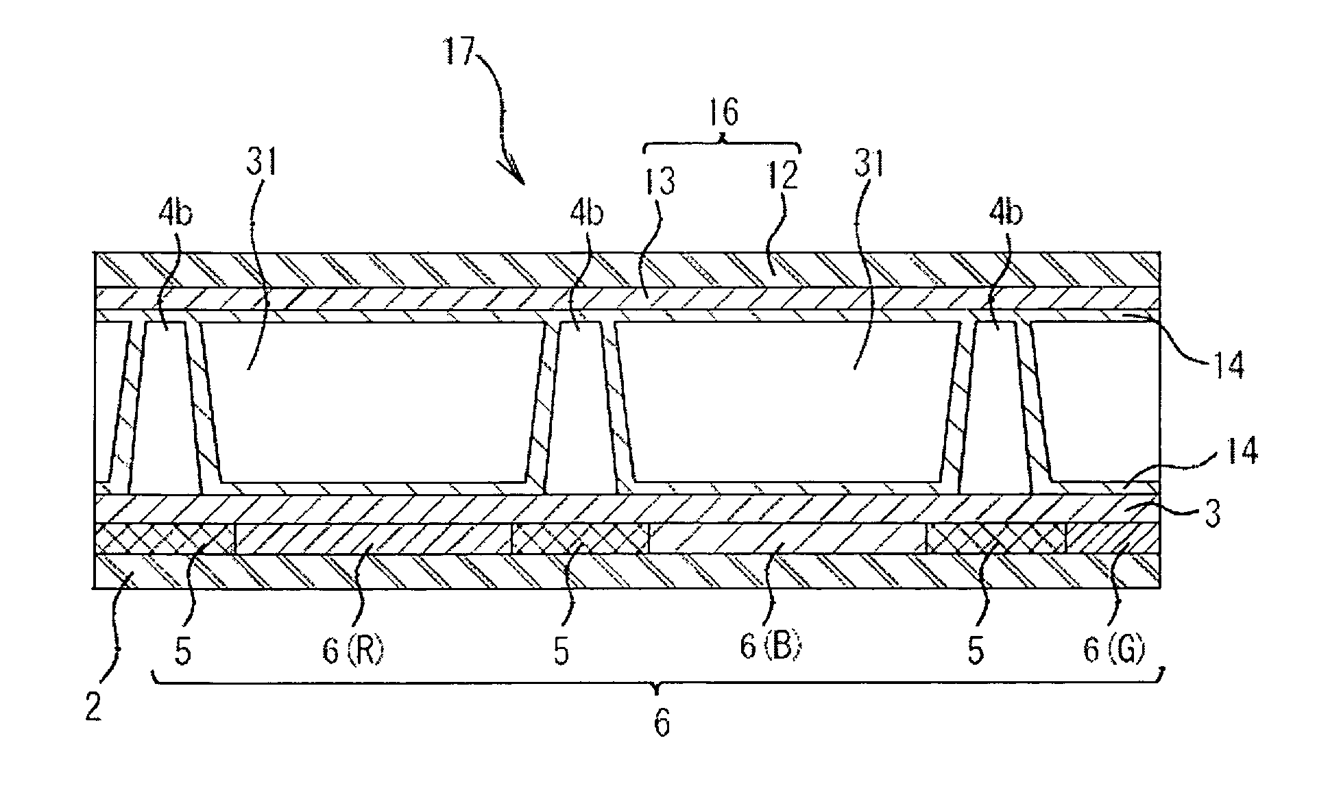
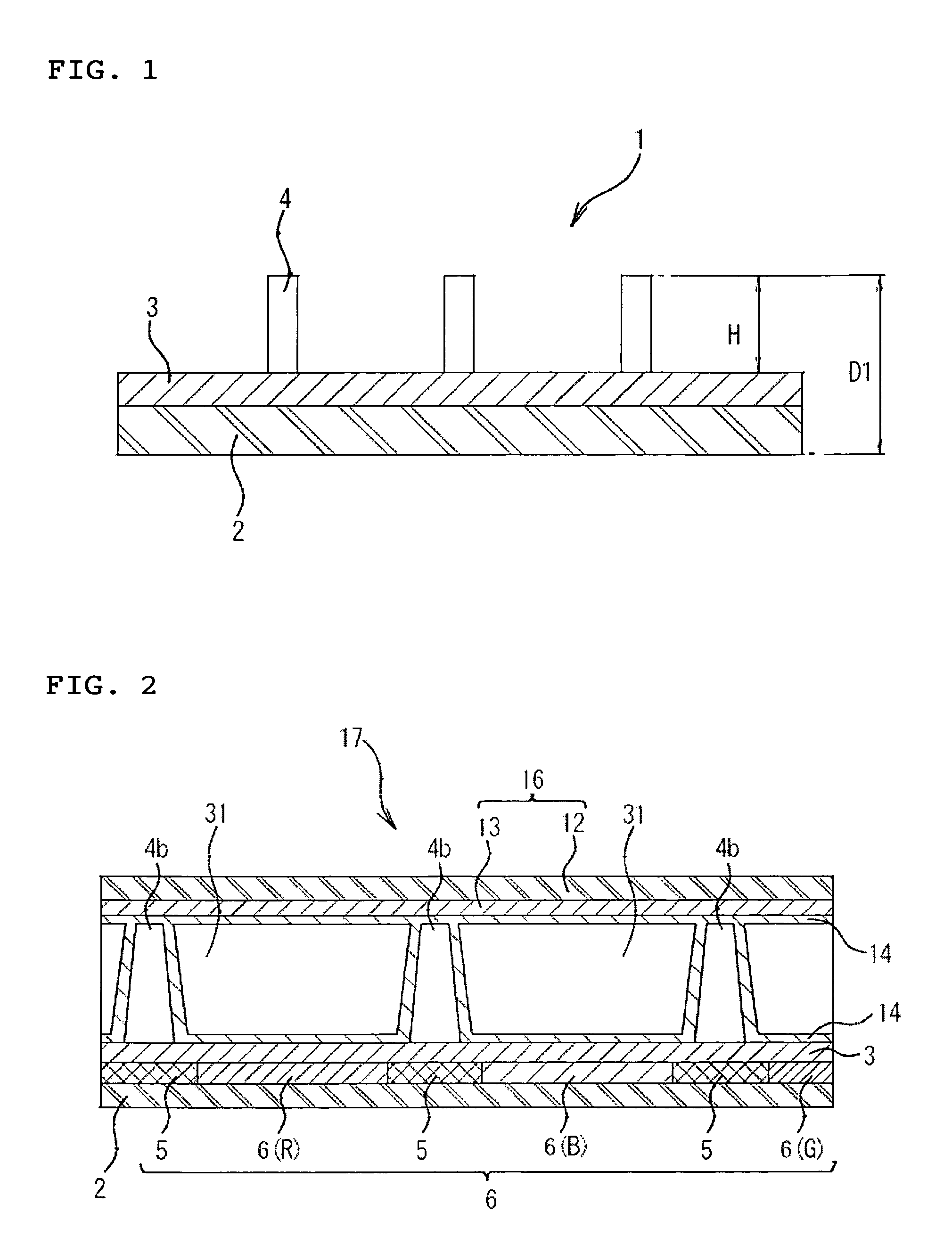
[0140]With alkali-free glass (trade name: NA35, produced by NH Technoglass Co., Ltd.) as a substrate, first, a light shielding region was formed, and then, transparent colored regions of red, green and blue color were formed between the light shielding regions by use of colored resists shown below according to a general photolithography process, thereby to constitute a colored layer having a thickness of substantially 2.0 μM.
[0141](Preparation of Colored Resist)
[0142]In order to form a light shielding region and transparent colored regions of three colors of red (R), green (G) and blue (B), pigment dispersion photoresists shown below were used as coloring materials. The pigment dispersion photoresist was obtained in such a manner that, with a pigment as a coloring material, beads were added to a dispersion composition (containing a pigment, a dispersing agent and a solvent), and the mixture was dispersed for 3 hr by a dispersing unit, followed by mixing a d...
example 2
[0198]In Example 2, a retardation-controlling optical member was formed in the same manner as in Example 1, except that a shape of a columnar structure was formed into a cylinder having a lower bottom surface of 12μφ; only 80,000 positions were selected per 100 cm2 on a retardation layer as positions scheduled to form columnar structures, without executing additive selection of one position to each of 80,000 positions; the number of the columnar structures disposed was set to 80,000 positions; and an occupation area rate of the lower bottom surface of the columnar structures to the surface area of the retardation layer was set to 0.36%.
reference examples 1 to 3
[0222]In Reference Example 1, a retardation-controlling optical member was formed in the same manner as in Example 1, except that a columnar structure was formed with taper such that a ratio of a cross sectional area of the columnar structure cut at a height of 90% from a lower bottom surface of the columnar structure to a lower bottom surface of the columnar structure (hereinafter, simply referred to as well as “90% height cross section ratio”) was set to 20%.
[0223]Similarly to Reference Example 1, a retardation-controlling optical member was formed as Reference Example 2 in the same manner as in Example 1 except that the 90% height cross section ratio was set to 3%, and a retardation-controlling optical member was formed as Reference Example 3 in the same manner as in Example 1 except that the 90% height cross section ratio was set to 70%.
[0224](Evaluation 3)
[0225]Loading and Unloading Test 2
[0226]In order to simulatively evaluate the securement of the margin when a retardation-co...
PUM
| Property | Measurement | Unit |
|---|---|---|
| transmittance | aaaaa | aaaaa |
| transmittance | aaaaa | aaaaa |
| thickness | aaaaa | aaaaa |
Abstract
Description
Claims
Application Information


