Method and system for encryption-based design obfuscation for an integrated circuit

a technology of encryption-based design and integrated circuit, which is applied in the direction of digital transmission, unauthorized memory use protection, instruments, etc., can solve the problems of certain percentage of manufactured devices failing prematurely, the development of integrated circuits (ics) has become increasingly complex, and the semiconductor industry is in the testing of manufactured chips

Inactive Publication Date: 2011-06-14
ATMEL CORP
View PDF11 Cites 4 Cited by
  • Summary
  • Abstract
  • Description
  • Claims
  • Application Information

AI Technical Summary

Benefits of technology

[0008]Aspects of encryption-based design obfuscation for an IC are described. Encryption-based design obfuscation for an integrated circuit includes creating multiple functional circuit paths for an integrated circuit design and selecting among the multiple functional circuit paths during scan testing. Encrypting selection data corresponding to an intended function of the integrated circuit design avoids revealing the intended function as a result of the scan testing.

Problems solved by technology

The development of integrated circuits (ICs) has become increasingly complex, due in large part to the ever increasing functionality offered by newly developed circuitry.
Regardless of the rigor of the developmental testing, invariably a certain percentage of manufactured devices will fail prematurely.
Thus, a problem existing in the semiconductor industry is in the testing of manufactured chips.
Even assuming a good, error-free logic design, it is well known that various faults and errors can enter into the production process, which can result in functional defects in a manufactured chip.
These faults can enter through a variety of causes in the numerous manufacturing process steps and can affect any of the different gates, switches or lines on the chip.
While such analysis tools can provide a level of assistance in isolating faults, they also create a level of vulnerability, since use of such tools allows for reverse engineering of the integrated circuit design.

Method used


Image

  • Method and system for encryption-based design obfuscation for an integrated circuit
  • Method and system for encryption-based design obfuscation for an integrated circuit

Examples


Embodiment Construction

[0012]The present invention relates to encryption-based design obfuscation for an integrated circuit. The following description is presented to enable one of ordinary skill in the art to make and use the invention and is provided in the context of a patent application and its requirements. Various modifications to the preferred embodiment and the generic principles and features described herein will be readily apparent to those skilled in the art. Thus, the present invention is not intended to be limited to the embodiments shown but is to be accorded the widest scope consistent with the principles and features described herein.

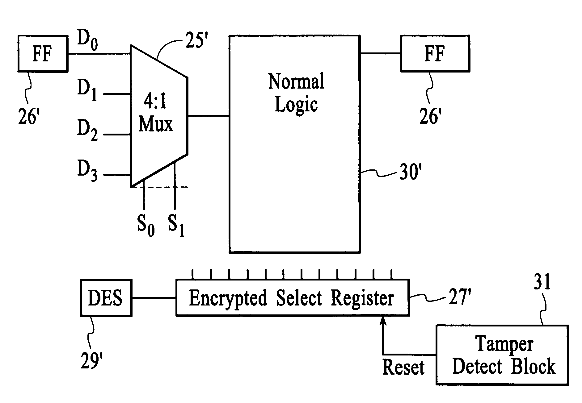
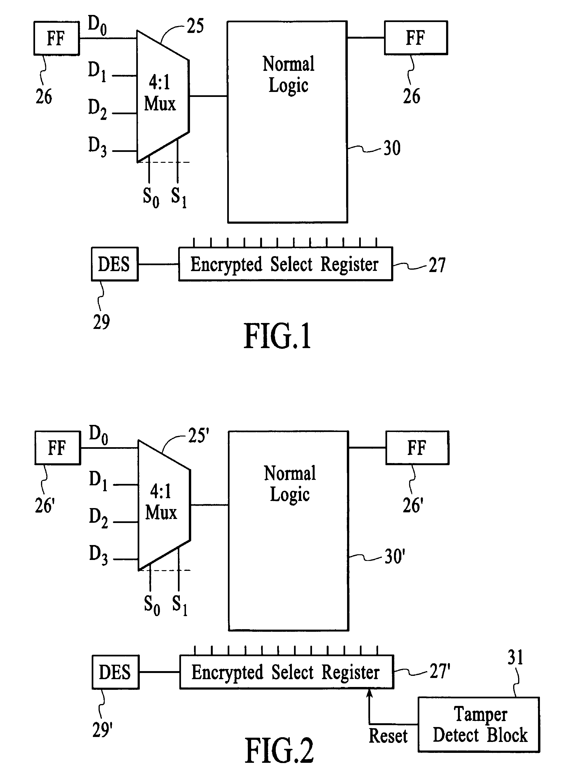
[0013]FIG. 1 illustrates a block diagram of encryption based design obfuscation for an integrated circuit that avoids revealing the design / reverse engineering as a result of scan testing in accordance with the present invention. A 4:1 MUX (multiplexer) 25 is inserted for use with every flip-flop 26 in the scan test. One input connection of MUX 25 is for the ac...


PUM


Abstract

Encryption-based design obfuscation for an integrated circuit includes creating multiple functional circuit paths for an integrated circuit design and selecting among the multiple functional circuit paths during scan testing. Encrypting selection data corresponding to an intended function of the integrated circuit design avoids revealing the intended function as a result of the scan testing.

Description

FIELD OF THE INVENTION[0001]The present invention relates to securing circuit design, and more particularly to encryption-based design obfuscation for integrated circuit designs.BACKGROUND OF THE INVENTION[0002]The development of integrated circuits (ICs) has become increasingly complex, due in large part to the ever increasing functionality offered by newly developed circuitry. Integrated circuits continue to surpass milestones in development, as more and more functionality is packaged into smaller sizes. This enhanced functionality and the greater number of transistors packaged in an integrated circuit requires more rigorous testing requirements to insure reliability once the device is commercialized. Thus, new integrated circuit designs are repeatedly tested and debugged during the development process to minimize the number and severity of errors that may subsequently arise. Regardless of the rigor of the developmental testing, invariably a certain percentage of manufactured devi...

Claims


Application Information

Patent Timeline
Patent Type & Authority Patents(United States)
IPC IPC(8): G06F11/30G06F12/14
CPCG01R31/318541H04L9/0625G01R31/318583H04L2209/16
Inventor FAGAN, JOHN
Owner ATMEL CORP
Why Eureka
Try Eureka