

Congestion aware pin optimizer
a pin optimizer and congestion-aware technology, applied in the field of integrated circuits and electronic design automation tools, can solve problems such as no solution, and achieve the effect of reducing routing congestion
- Summary
- Abstract
- Description
- Claims
- Application Information
AI Technical Summary
Benefits of technology
Problems solved by technology
Method used
Image

Examples
exemplary embodiment 200
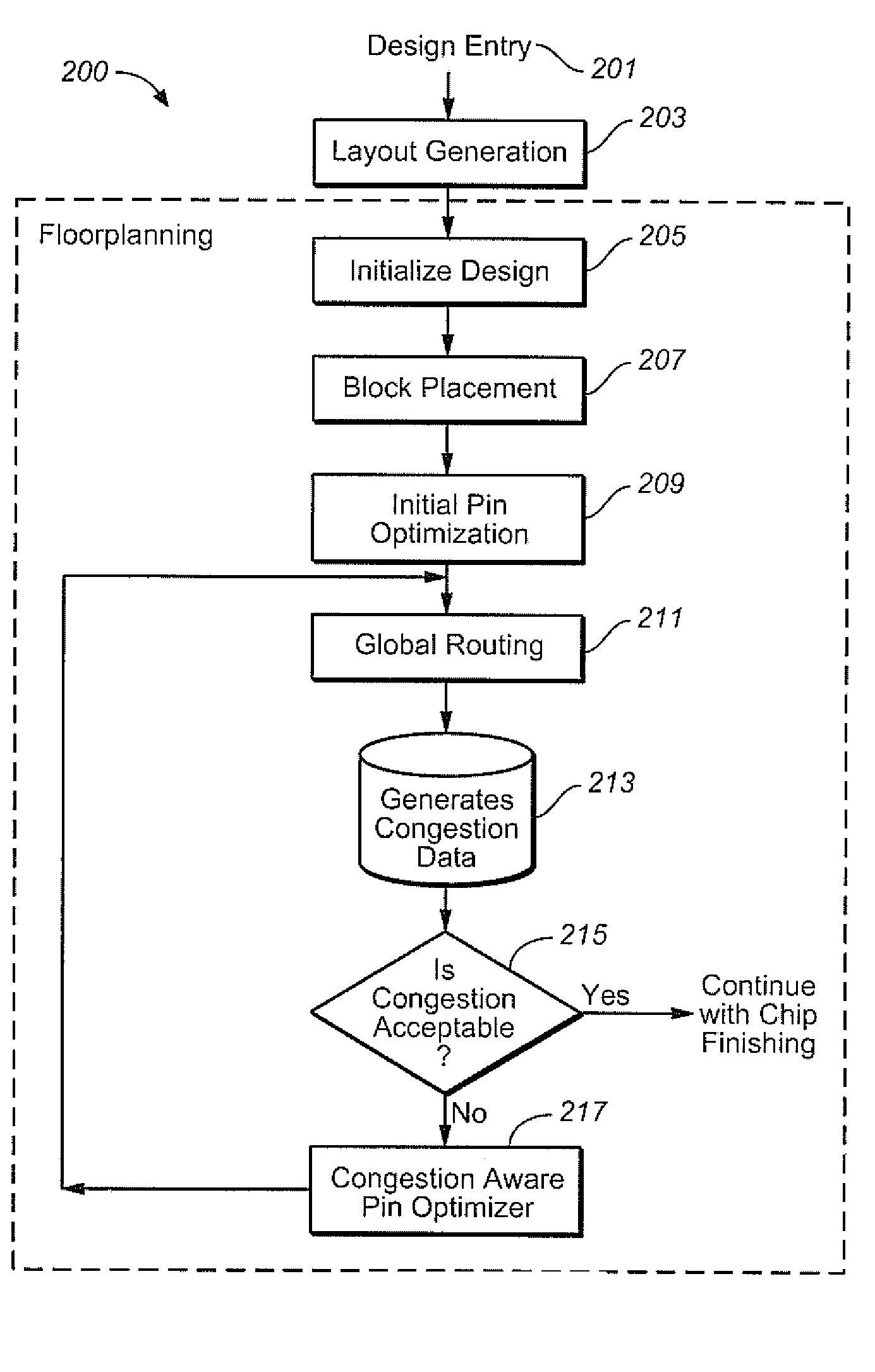
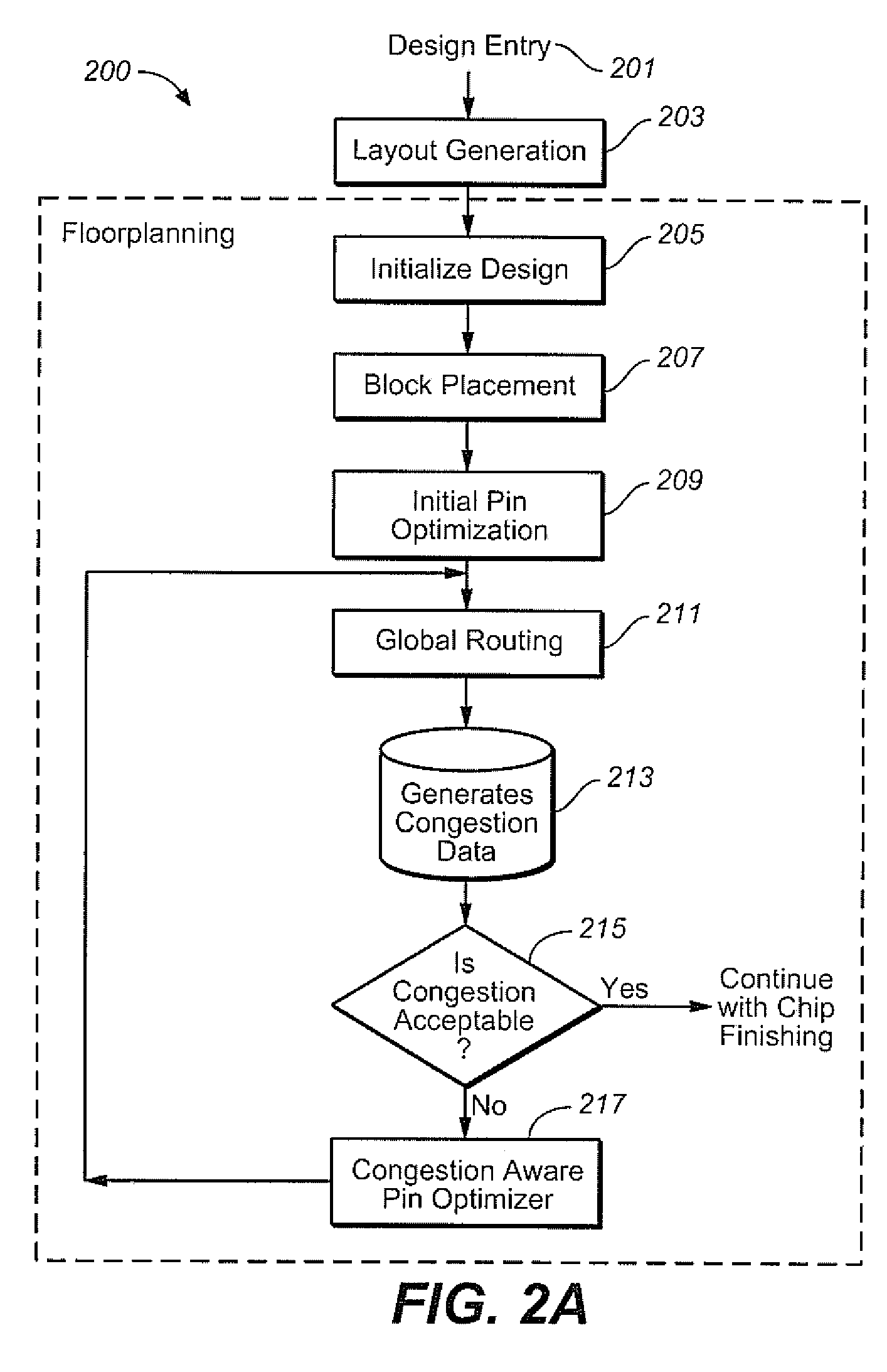
[0027]FIG. 2A shows an exemplary embodiment 200 for a congestion aware pin optimization flow, beginning with design entry at 201. Once the layout is generated at 203, the design is initialized at 205 and block placement 207 is done so that blocks are placed inside the design boundary. After block placement, the initial pin optimization 209 is run, and congestion data is generated 213 during global routing 211. Congestion data is then analyzed at 215, and if there are high congestion areas in the design (No from 215), then pin optimizer 217 is run in congestion aware mode to reposition pins and reduce the congestion.
[0028]The determination of whether there are high congestion areas can be done by analyzing if there are highly congested “GCells”. In this exemplary embodiment, the global router can present the congestion data in terms of GCells and a congestion map. A congestion map is a two dimensional grid (possibly non-uniform) that exists for each layer in the design. Each Grid cel...
case 1
[0063] Congestion is Higher in Vertical Direction in a GCell
[0064]If the congestion is high in vertical direction, then the routing blockage is created in the vertical direction so that a lesser number of pins can be assigned in that GCell, thereby reducing congestion. For example, if the target congestion value is CT and the actual congestion value is CA in a particular GCell, then the dimensions of routing blockage are computed as shown in FIG. 8.
[0065]FIG. 8 illustrates weighted blockage creation in vertical direction for a GCell of width w and height h. Here,
Weighted Blockage width=GCell width×(1−CT / CA); and
Weighted Blockage height=GCell height.
If, for example, CA=100 and CT=50, then:
Weighted Blockage width=w×(1−50 / 100), or w / 2; and
Weighted Blockage height=h,
as are shown on the right hand side of FIG. 8.
case 2
[0066] Congestion is Higher in Horizontal Direction in a GCell
[0067]If the congestion is high in the horizontal direction, then the routing blockage is created in horizontal direction, so that a lesser number of pins can be assigned in that GCell, thereby reducing congestion. As in Case 1, if the target congestion value is CT and the actual congestion value is CA in a particular GCell, then the dimensions of routing blockage are computed as shown in FIG. 9.
[0068]FIG. 9 again illustrates weighted blockage creation in vertical direction for a GCell of width w and height h. Here,
Weighted Blockage height=GCell height×(1−CT / CA); and
Weighted Blockage width=GCell width.
If, for example, CA=100 and CT=50, then:
Weighted Blockage height=h×(1−50 / 100), or h / 2; and
Weighted Blockage width=w,
as shown on the right hand side of FIG. 9.
Congestion Aware Pin Optimization
[0069]Applying the above formula on the design of FIG. 4, routing blockages will be modeled as shown in FIG. 10. As shown in FIG. 10A,...
PUM
 Abstract
Description
Claims
Application Information