Adaptive bias technique for field effect transistor

a field effect transistor and biasing technology, applied in the direction of amplifiers, amplifiers with semiconductor devices only, amplifiers with semiconductor devices, etc., can solve the problems of significant variation in system-wide modulation schemes that employ complex modulation schemes, and limited bandwidth of the transmitting system, so as to achieve the effect of reducing the envelope of the transmitted signal

Active Publication Date: 2011-07-26
LEHIGH UNIVERSITY
View PDF7 Cites 31 Cited by
  • Summary
  • Abstract
  • Description
  • Claims
  • Application Information

AI Technical Summary

Problems solved by technology

Modern communication systems employ complex modulation schemes to achieve high data rates within a limited bandwidth.
These techniques result in significant variation in the envelope of the transmitted signal.
Even with modulation schemes where the information is only embedded in the phase of the carrier, like QPSK and OFDM, the limited bandwidth of the transmitting system leads to variations in the envelope of the signal.
The high peak-to-average ratio is a problem for the efficient operation of power amplifiers described above, which have to operate at reduced power levels in order to transmit the peak signals with acceptable linearity.
However, increasing the shielding electrode voltage with the drain voltage fixed at its typical quiescent value of 28V leads to a faster degradation of the on-resistance.

Method used


Image

  • Adaptive bias technique for field effect transistor
  • Adaptive bias technique for field effect transistor
  • Adaptive bias technique for field effect transistor

Examples


Embodiment Construction

[0022]This description of the exemplary embodiments is intended to be read in connection with the accompanying drawings, which are to be considered part of the entire written description.

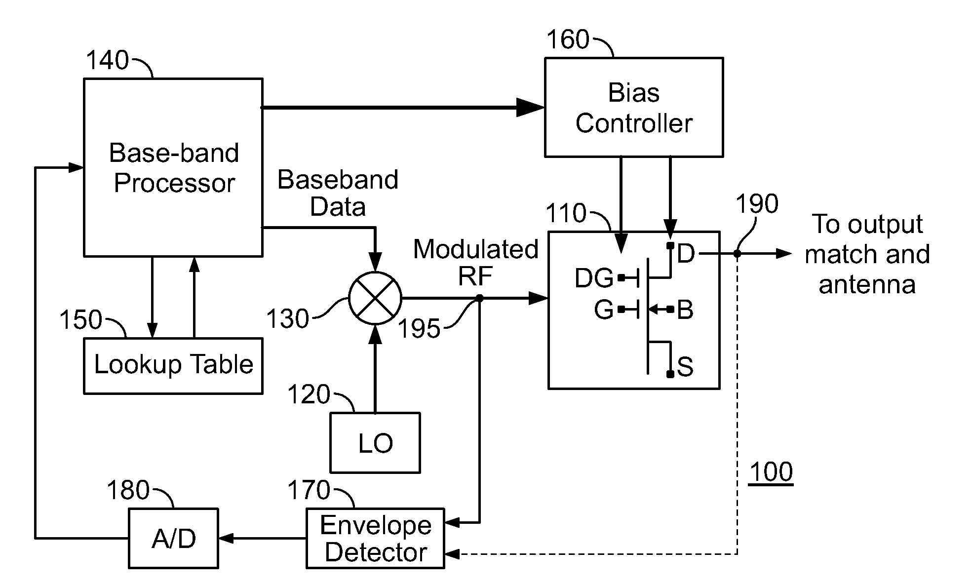
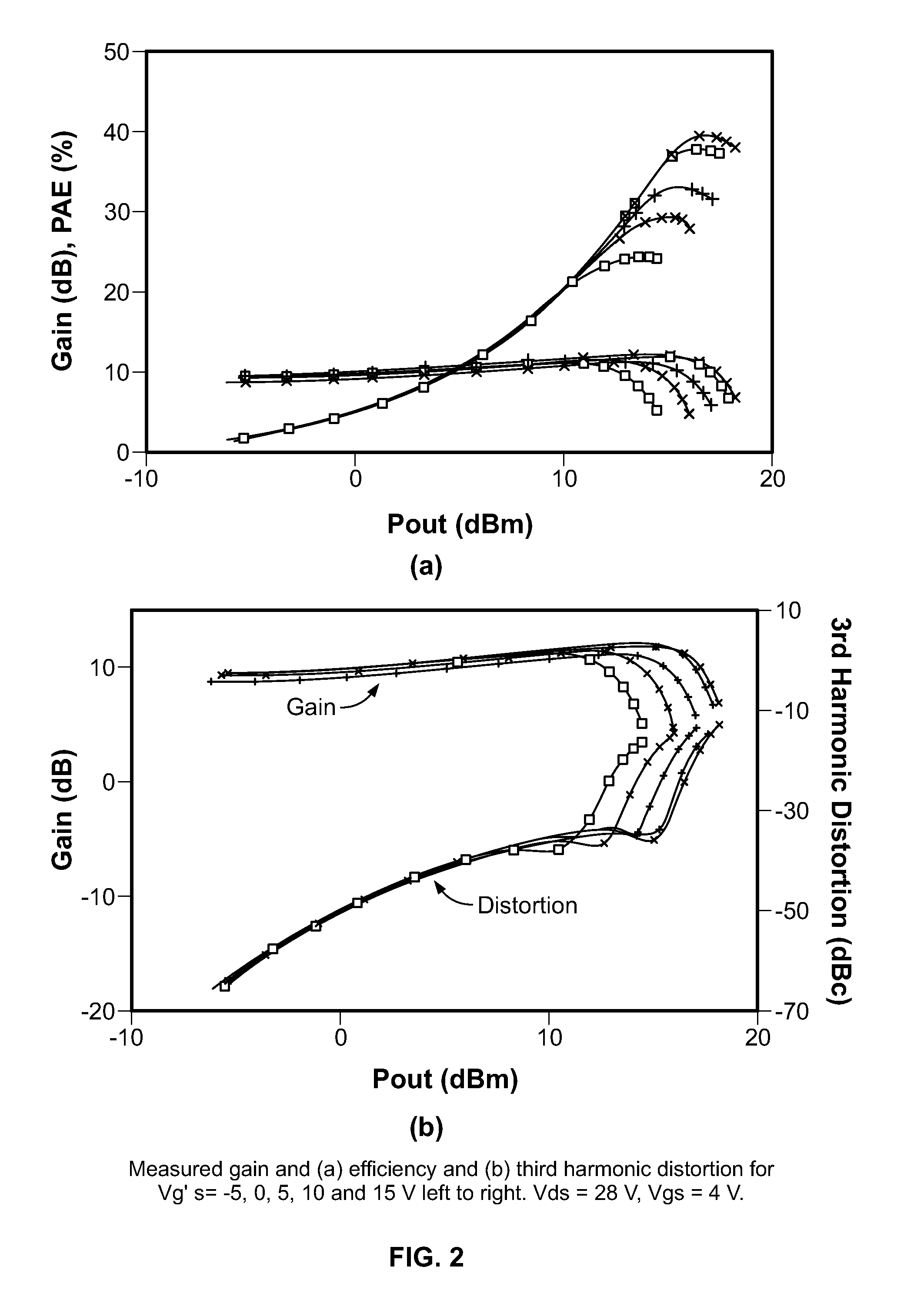
[0023]Techniques for adaptive biasing of LDMOS power transistors to improve the overall output power, efficiency, linearity and reliability are described herein. In exemplary embodiments, both the shielding electrode (which in embodiments is, by way of example, a dummy gate, shield plate or buried shield plate (collectively “shielding electrode”)) and the drain are adaptively biased based on RF signal power information for the input or output RF signal.

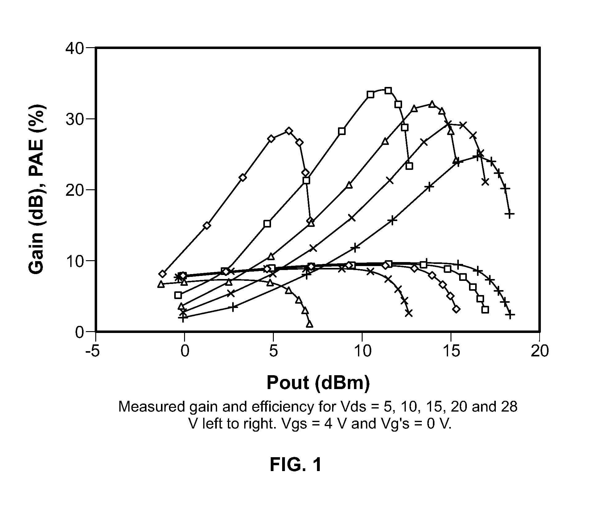
[0024]In adaptive drain biasing systems, the quiescent drain voltage is modulated according to the envelope of the RF signal. For a fixed load ROPT, different quiescent drain voltages will have different maximum voltage and current swings. So, the maximum drain voltage and current swings are functions of the quiescent drain voltage Vds. LDMOS based po...


PUM


Abstract

A power amplifier includes a LDMOS transistor having a source, a drain, a control gate and a shielding electrode positioned between the control gate and the drain, and means for adaptively biasing the drain and shielding electrode power information for a RF signal.

Description

CROSS-REFERENCE TO RELATED APPLICATIONS[0001]This application claims priority to U.S. Provisional Patent Application No. 60 / 870,173 to Marvin Marbell and James Hwang, entitled “Adaptive Bias Technique for Field-Effect Transistors”, filed Dec. 15, 2006, the entirety of which is hereby incorporated by reference herein.FIELD OF THE INVENTION[0002]The present invention relates to power field effect transistors and more particularly to power LDMOS transistors.BACKGROUND OF THE INVENTION[0003]Modern communication systems, such as cellular communication systems, utilize laterally diffused MOS transistors (LDMOS) as power amplifiers. LDMOSs have high voltage handling capacity made possible by the lightly doped drain (LDD) between the drain contact and the active channel. The LDD increases breakdown voltage at the expense of increased drain resistance. Extending the gate or drain electrode over the LDD decreases the drain resistance but increases the gate-drain and gate-source capacitances. ...

Claims


Application Information

Patent Timeline
Patent Type & Authority Patents(United States)
IPC IPC(8): H03F3/20
CPCH03F1/0222H03F1/0266
Inventor MARBELL, MARVIN NII NARTEYHWANG, JAMES CHENG-MIN
Owner LEHIGH UNIVERSITY
Why Eureka
Try Eureka