Method of forming stacked-die integrated circuit

a technology of integrated circuits and dies, applied in semiconductor devices, semiconductor/solid-state device details, electrical apparatus, etc., can solve the problems of insufficient mechanical robustness of mother and daughter connection, small array of contact pads and solder bumps than the mother die, and new challenges of stacking di

Active Publication Date: 2011-08-02
XILINX INC
View PDF33 Cites 32 Cited by
  • Summary
  • Abstract
  • Description
  • Claims
  • Application Information

AI Technical Summary

Benefits of technology

[0008]In one embodiment, the stacked-die integrated circuit is mounted to a packaging substrate that provides connectivity between the integrated circuit and the outside environment. This allows the entire package to be mechanically robust without alteration of mother die and daughter die circuitry.

Problems solved by technology

Stacking dice, though, brings new challenges.
A daughter die typically has fewer total connection points to its circuitry than does the mother die, resulting in a smaller array of contact pads and solder bumps than the mother die.
Often, this means that the connection between mother and daughter, though electrically sound, is insufficiently robust mechanically.
This complicates the handling and processing of the mother / daughter assembly during packaging and other processing.

Method used


Image

  • Method of forming stacked-die integrated circuit
  • Method of forming stacked-die integrated circuit
  • Method of forming stacked-die integrated circuit

Examples


Embodiment Construction

[0021]In the following description, numerous specific details are set forth to provide a more thorough description of the specific embodiments of the invention. It should be apparent, however, to one skilled in the art, that the invention may be practiced without all the specific details given below. In other instances, well known features have not been described in detail so as not to obscure the invention. For ease of illustration, the same number labels are used in different diagrams to refer to the same items; however, in alternative embodiments the items may be different.

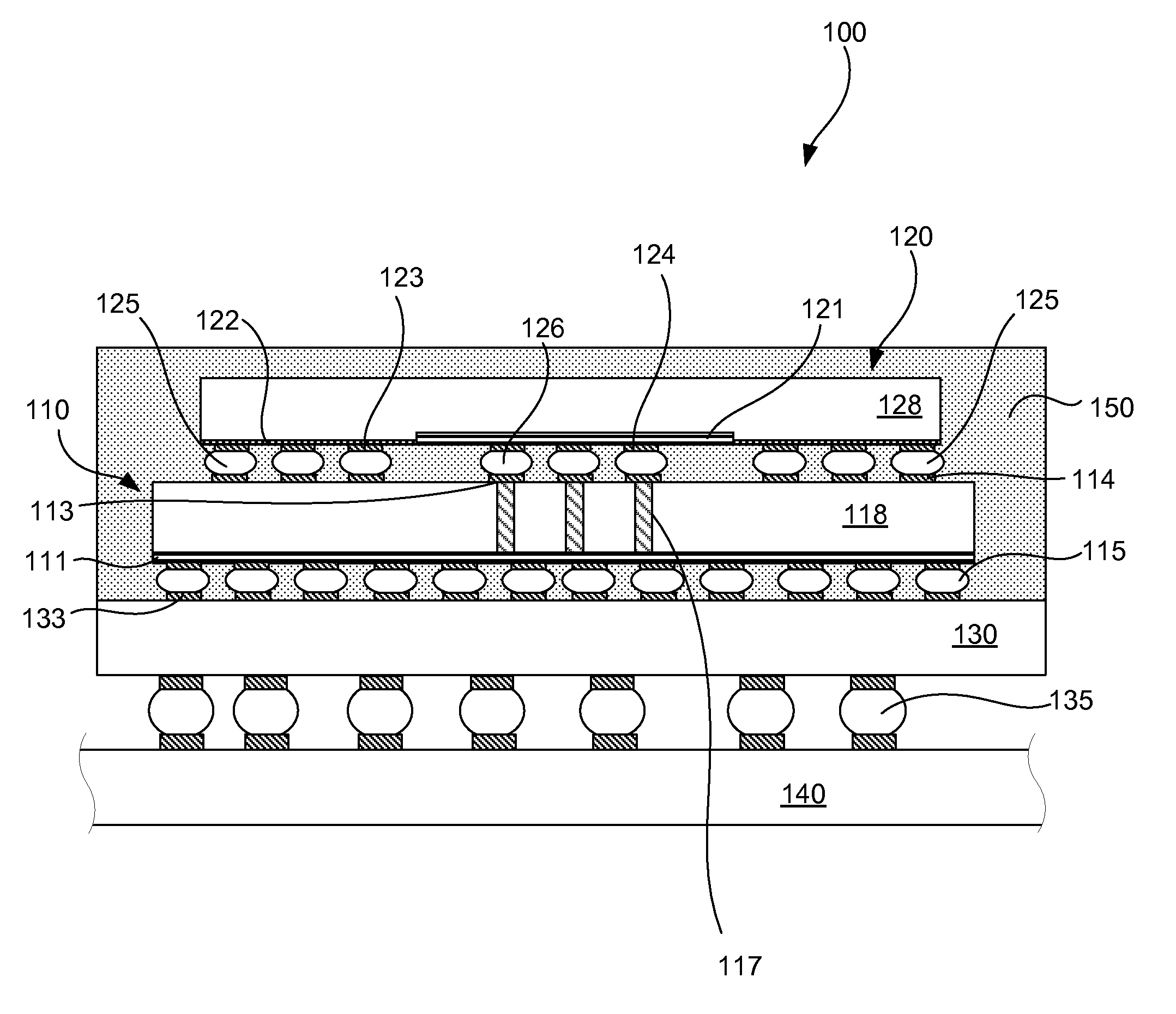
[0022]FIG. 1 illustrates a packaged and mounted stacked-die semiconductor device in accordance with an embodiment of the present invention. Semiconductor device 100 comprises mother die 110, daughter die 120, and package substrate 130. The assembly is typically encapsulated in a packaging material 150. The packaging material is typically an epoxy or other thermosetting material that provides electrical insulati...


PUM


Abstract

A stacked-die integrated circuit and a method of fabricating same. The stacked-die integrated circuit has circuitry formed in the first surface of a mother die, a plurality of through-die vias with at least one through-die via providing electrical connection between the circuitry of the mother die and the second surface and a plurality of contact pads formed in the second surface of the semiconductor die for mounting a daughter die wherein some of the contact pads are electrically isolated dummy pads.

Description

FIELD OF THE INVENTION[0001]The present application relates generally to integrated circuits, and in particular, to a stacked-die integrated circuit device package and methods of forming the same.BACKGROUND OF THE INVENTION[0002]Modern integrated circuit devices continue to shrink in size as they accelerate in speed. More and more functionality is demanded of less and less device “real estate” or available circuit space, whether on the printed circuit board of an electronic appliance or on the semiconductor chip in which integrated circuits are formed.[0003]Existing integrated circuits are essentially two-dimensional in that they are formed on the surface of flat semiconductor wafers. Until the advent of the stacked-die assembly, notwithstanding the development of limited multi-layer circuitry, the only ways to increase the complexity of a circuit were to increase the area of semiconductor used or to shrink feature size.[0004]Stacked die technology has taken semiconductor fabricatio...

Claims


Application Information

Patent Timeline
Patent Type & Authority Patents(United States)
IPC IPC(8): H01L23/42H01L21/44
CPCH01L23/3128H01L23/481H01L24/06H01L24/14H01L25/0657H01L21/563H01L2924/0002H01L2224/0557H01L2224/0603H01L2224/06132H01L2224/06519H01L2224/14132H01L2224/14135H01L2224/14136H01L2224/14177H01L2224/14515H01L2224/16H01L2225/06513H01L2225/06517H01L2225/06541H01L2225/06589H01L2924/014H01L2924/15311H01L2224/05554H01L2224/0401H01L2224/05552H01L2224/16145H01L2224/16225H01L2224/17181H01L2924/14H01L2924/00
Inventor RAHMAN, ARIFUR
Owner XILINX INC
Why Eureka
Try Eureka