MRAM device with shared source line

a random access memory and source line technology, applied in information storage, static storage, digital storage, etc., can solve the problems of low array density resulting from bit line and source line spacing, source lines cannot be connected to ground nor shared across an entire array, and conventional stt-mram devices. achieve the effect of reducing device area, less device area, and increasing array density

Active Publication Date: 2011-08-09
QUALCOMM INC
View PDF13 Cites 20 Cited by
  • Summary
  • Abstract
  • Description
  • Claims
  • Application Information

AI Technical Summary

Benefits of technology

[0009]One particular advantage provided by the disclosed embodiments is reduced device area. Fewer lines are required to access cells of a MTJ memory array and therefore less device area is reserved for separation between lines. Array density may be increased since fewer lines are required. Another advantage is simplified source line routing due to a reduced number of source lines. The MRAM devices of the disclosed embodiments may be smaller than comparable SRAM devices and may be less expensive to manufacture. In addition, the MRAM devices of the disclosed embodiments may be faster than comparable flash memory devices.

Problems solved by technology

One limitation of conventional STT-MRAM devices is low array density resulting from bit line and source line spacing due to the source line configuration in the memory array.
Because STT-MRAM uses bidirectional current to write complementary data, source lines cannot be connected to ground nor shared across an entire array, as is possible in other memory technologies.

Method used


Image

  • MRAM device with shared source line
  • MRAM device with shared source line
  • MRAM device with shared source line

Examples


Embodiment Construction

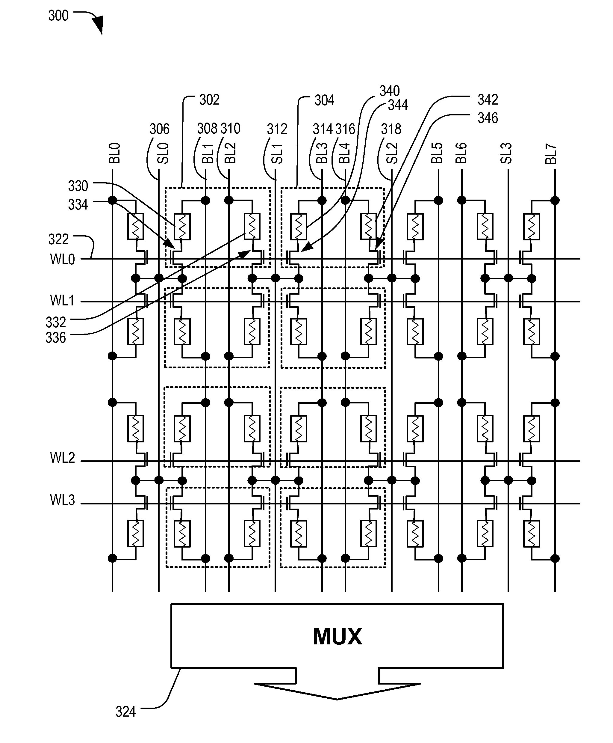
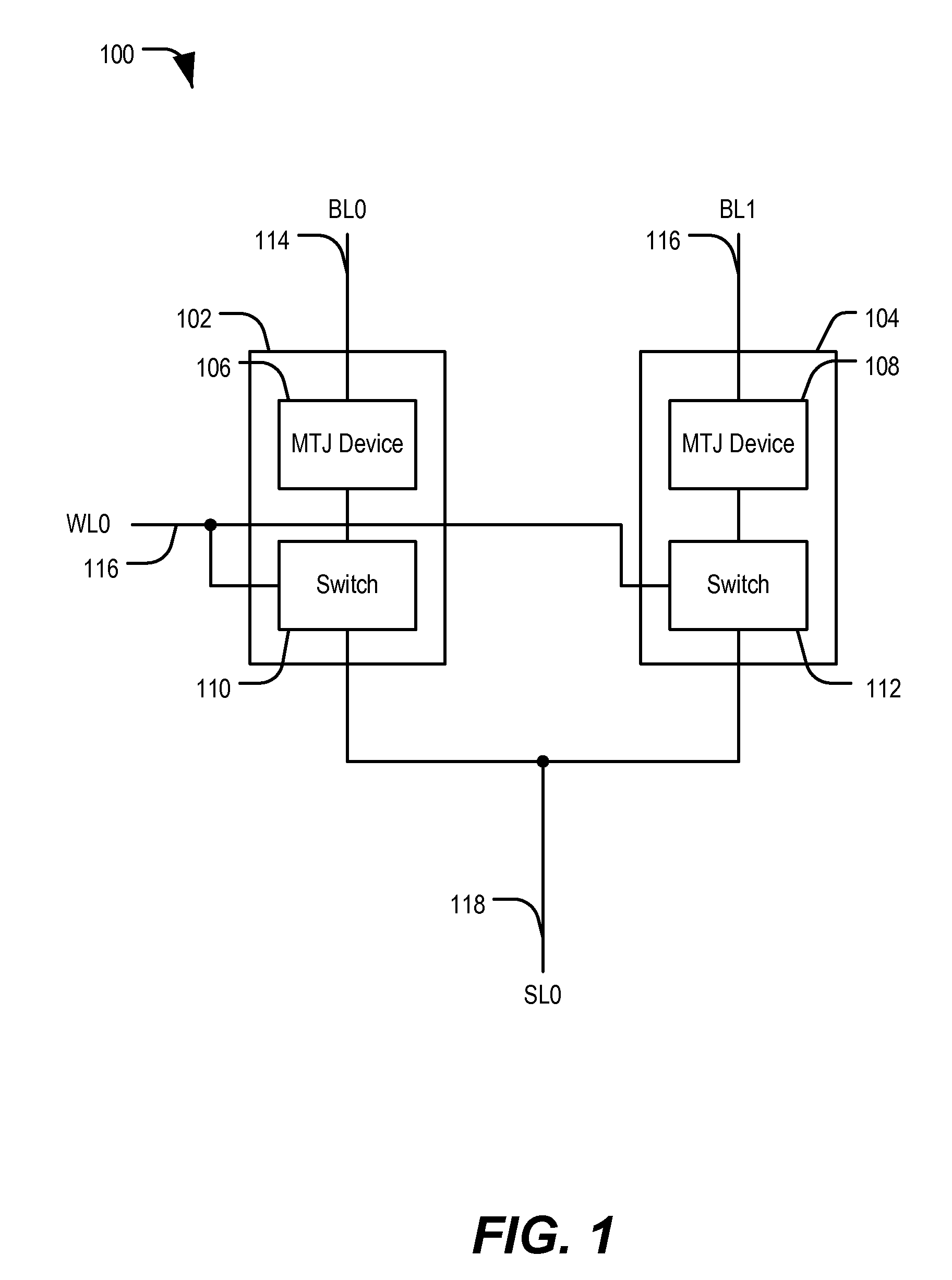
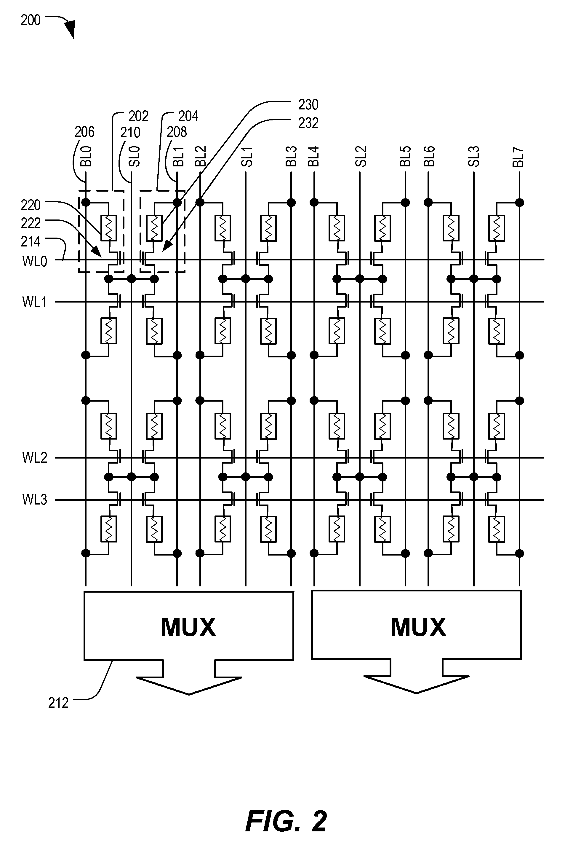
[0016]Referring to FIG. 1, a block diagram of a particular illustrative embodiment of an MRAM device with a shared source line is depicted and generally designated 100. The device 100 includes a first representative memory cell 102 and a second representative memory cell 104. A first bit line (BL0) 114 is coupled to the first memory cell 102. A second bit line (BL1) 116 that is distinct from the first bit line 114 is coupled to the second memory cell 104. A shared source line (SL0) 118 is coupled to the first memory cell 102 and to the second memory cell 104. A word line (WL0) 116 is coupled to the first memory cell 102 and the second memory cell 104.

[0017]The first memory cell 102 includes a magnetic tunnel junction (MTJ) device 106 coupled to the first bit line 114. The MTJ device 106 is also coupled to a switch 110, such as a transistor. The switch 110 is configured to selectively couple the MTJ device 106 to the source line 118 in response to a control signal received via the wo...


PUM


Abstract

In a particular embodiment, a memory device includes a first memory cell and a second memory cell. The memory device also includes a first bit line associated with the first memory cell and a second bit line associated with the second memory cell. The memory device also includes a source line coupled to the first memory cell and coupled to the second memory cell.

Description

I. FIELD[0001]The present disclosure is generally related to a magnetoresistive random access memory (MRAM) device having a shared source line.II. DESCRIPTION OF RELATED ART[0002]Conventional spin transfer torque magnetoresistive random access memory (STT-MRAM) bit cells include a transistor and a magnetic tunnel junction (MTJ) structure. The basic MTJ structure consists of two magnetic electrodes sandwiching a tunnel barrier layer. The magnetic moment of each magnetic electrode is oriented along a long axis of an elongated element. The parallel and anti-parallel magnetic moment orientation between the two magnetic layers on either side of the tunnel barrier gives rise to two different resistances across the barrier, resulting in two memory states. One of the magnetic electrodes has a magnetic moment direction that can be switched based on an applied current density and direction. The other magnetic electrode has a magnetization that is pinned to a particular direction.[0003]Convent...

Claims


Application Information

Patent Timeline
Patent Type & Authority Patents(United States)
IPC IPC(8): G11C11/00
CPCG11C11/16G11C11/1659G11C11/1673G11C11/1675
Inventor YOON, SEI SEUNGZHONG, CHENGPARK, DONGKYUABU-RAHMA, MOHAMED H.
Owner QUALCOMM INC
Why Eureka
Try Eureka