Display apparatus and driving method thereof

a technology of display apparatus and driving method, which is applied in the direction of static indicating device, electroluminescent light source, instruments, etc., can solve the problems of difficult implementation of image display apparatus having a large size and high degree of fineness, and achieve the reduction of the number of components composing the pixel circuit, the reduction of the number of power supply lines and the number of gate lines (or scanning lines), and the reduction of the number of crossovers between wires.

Inactive Publication Date: 2011-08-23
SONY CORP
View PDF12 Cites 17 Cited by
  • Summary
  • Abstract
  • Description
  • Claims
  • Application Information

AI Technical Summary

Benefits of technology

[0008]The input voltage held by the capacitor is supplied to the gate of the drive transistor, causing the output current to flow to the light emitting device through the source and drain of the drive transistor. In general, the luminance of the light emitted by the light emitting device is proportional to the magnitude of the current output by the drive transistor to the device, and the magnitude of the current is controlled by the input voltage held by the capacitor and applied to the gate of the transistor. In the conventional pixel circuit, by changing the input voltage applied to the gate of the drive transistor in accordance with the input video signal, the magnitude of the current flowing to the light emitting device can be controlled.
[0025]In accordance with an embodiment of the present invention, the image display apparatus has a threshold-voltage compensatory function embedded in each pixel circuit. In a horizontal scanning period (1H) allocated to each row of pixels, the image display apparatus carries out a threshold-voltage compensation preparatory operation, an actual threshold-voltage compensatory operation and an operation to sample the voltage of a video signal by making use of an effect of gate coupling. Thus, the number of components composing the pixel circuit can be reduced. To put it concretely, the pixel circuit provided by the present invention includes only three transistors, one pixel capacitor and one light emitting device. As a result, the number of power-supply lines and the number of gate lines (or scanning lines) can also be reduced so that the number of crossovers between wires can be decreased substantially. Accordingly, the yield of a panel forming the image display apparatus can be improved and, at the same time, the degree of panel fineness can also be raised as well. In addition, in accordance with an embodiment of the present invention, besides a sampling operation, a compensatory operation can also be carried out during a horizontal scanning period. Thus, in addition to a signal electric potential, a fixed electric potential for a control purpose can also be provided on same data signal line as the signal electric potential. In this way, the image display apparatus according to the present invention is capable of providing the pixel-array unit with not only image data through the data signal line, but also a fixed voltage through the same data signal line as a voltage for controlling the pixel circuit. Thus, by using only a small number of components, it is possible to implement a compensatory unit configured to compensate each of pixel circuits for an effect of the variations in characteristics among drive transistors employed in different pixel circuits. In addition, even if the fixed voltage for controlling the pixel circuit is higher than a maximum rating voltage of an ordinary driver IC serving as a signal unit for generating the signal appearing on the data signal line, only an output circuit of the driver IC needs to be made tolerable against the high fixed voltage. That is to say, it is not necessary to make the entire driver IC tolerable against the high fixed voltage. Thus, it is possible to prevent the cost of the driver IC from rising due to the increasing physical size of the driver IC as encountered in an effort to enlarge the scale of image display apparatus or increase the pitch between pins of the driver IC. As a result, the image display apparatus is capable of keeping up with a panel having a high resolution.
[0026]In addition, in accordance with an embodiment of the present invention, the scanner unit employed in the image display apparatus outputs control signals to their respective scanning lines during a horizontal scanning period in order to control pixel circuits. The pixel circuit is controlled in this way in order to carry out following operations. These operations are: a compensatory operation of compensating a pixel capacitor employed in the pixel circuit for an effect of a characteristic exhibited by an output current of a drive transistor employed in the pixel circuit as a characteristic of dependence on the threshold voltage of the drive transistor; and a sampling operation of sampling the electric potential of a video signal supplied by a signal unit to a signal line and storing the sample electric potential in the compensated pixel capacitor. At that time, the scanner unit utilizes previous horizontal scanning periods each allocated to a row of pixels preceding the current row of pixels to carry out the compensatory operation to compensate the pixel capacitor at different times by distributing the compensatory operation among the previous horizontal scanning periods. By distributing the compensatory operation, which is to be carried out to compensate the pixel capacitor for the effect of a characteristic exhibited by an output current of a drive transistor employed in the pixel circuit as a characteristic of dependence on the threshold voltage of the drive transistor, among a plurality of horizontal scanning periods in this way, a sufficiently long compensation period can be assured. This is because results of the compensatory operation distributed among a plurality of horizontal scanning periods can be accumulated so that, when the operation to sample a video signal is carried out in a horizontal scanning period eventually, an adequate voltage corresponding to the threshold voltage of a drive transistor has been stored in the pixel capacitor. As a result, it is possible to carry out a sufficient compensatory operation of compensating the pixel capacitor for the effect of a characteristic exhibited by an output current of the drive transistor employed in the pixel circuit as a characteristic of dependence on the threshold voltage even if the driving frequency of the image display apparatus is increased, resulting in short horizontal scanning periods.
[0027]In particular, in accordance with an embodiment of the present invention, the image display apparatus carries out a threshold-voltage compensation preparatory operation, an actual threshold-voltage compensatory operation and an operation to sample the voltage of a video signal in a horizontal scanning period. By carrying out necessary operations during a horizontal scanning period in this way, necessary video-signal and control voltages are supplied to the pixel circuit by a signal unit through the signal line. Thus, the pixel circuit can be designed to include only a small number of components. By the way, the pixel circuit provided by the present invention has only three transistors, one pixel capacitor and one light emitting device. Thus, the number of components composing the pixel circuit is very small in comparison with the conventional pixel circuit having a threshold-voltage compensation function. In order to carry out an actual threshold-voltage compensatory operation and an operation to sample the voltage of a video signal in a horizontal scanning period; however, it may be impossible to assure a needed sufficiently long operating time in case the horizontal scanning period becomes short due to an increased driving frequency. In order to solve this problem, the present invention carries out the threshold-voltage compensation preparatory operation in a plurality of horizontal scanning periods by distributing the threshold-voltage compensation preparatory operation among the horizontal scanning periods. Then, results of the compensatory operation distributed among the horizontal scanning periods are accumulated so that, in essence, it is possible to assure the needed sufficiently long operating time.
[0028]In accordance with an embodiment of the present invention, the threshold-voltage compensation preparatory operation is carried out by making use of an effect of capacitive coupling. The threshold-voltage compensation preparatory operation making use of an effect of capacitive coupling is carried out a plurality of times. The interval between any two consecutive pulses triggering two consecutive threshold-voltage compensation preparatory operations is set at a value large enough for discharging a voltage from the light emitting device. In this way, the number of minus coupling operations per row can be reduced. In the present invention, the interval between two consecutive driving control pulses applied to the gate of the sampling transistor in order carry out a threshold-voltage compensation preparatory operation is set at such a value that the light emitting device is fully cut off at the end of the interval. By carrying out this threshold-voltage compensation preparatory operation repeatedly a number of times, an effect of the variations in gate electric potential disappears so that it is possible to obtain a needed voltage to be applied between the gate and source of a drive transistor. By setting the interval between any two consecutive pulses triggering two consecutive threshold-voltage compensation preparatory operations at a sufficiently large value in this way, the number of pulses each triggering a threshold-voltage compensation preparatory operation can be considerably reduced to a value, which is small in comparison with the conventional pixel circuit. In accordance with an embodiment of the present invention, in an organic EL panel with light emitting devices each having a large capacitance or in a panel similar to such a panel, the threshold-voltage compensation period is split into a plurality of sub-periods and the interval between any two consecutive driving control pulses each triggering a threshold-voltage compensation operation is set at such a value that the light emitting device is fully cut off at the end of the interval. Thus, the number of pulses each triggering a threshold-voltage compensatory operation can be considerably reduced to a value small.
[0029]In addition, in accordance with an embodiment of the present invention, the scanner unit employed in the image display apparatus as a unit for sequentially scanning rows of pixels executes control of turning on and off the sampling and switching transistors included in each pixel circuit in order to carry out a compensatory operation to compensate the pixel capacitor for an effect of the threshold voltage of the drive transistor and an operation to sample a video signal. In this way, the image display apparatus is capable of suppressing the effect of variations in threshold voltage among drive transistors employed in different pixel circuits. Thus, it is possible to obtain a uniform picture quality without unevenness and variations. In addition, the pixel capacitor employed in each pixel circuit applies an input voltage according to the electric potential of a sampled video signal between the gate and source of the drive transistor. Since the pixel capacitor sustains the electric potential applied between the gate and source of the drive transistor at a constant value, the drive transistor works as a constant current generator supplying a constant output current to the light emitting device. Thus, even if the I-V characteristic of the light emitting device deteriorates with the lapse of time, the constant output current keeps flowing to the light emitting device all the time, causing the device to emit a light beam at a constant luminance according to the sampled video signal. The pixel circuit capable of coping with variations in characteristics among different drive transistors and deteriorations of the I-V characteristic of the light emitting device with the lapse of time in this way can be configured to include only a sampling transistor, a switching transistor, a drive transistor and a pixel capacitor. Thus, the pixel circuit employed in the image display apparatus provided by the present invention has a configuration including only four components, i.e., three transistors and one capacitive element. Since the number of components (that is, the three transistors and the pixel capacitor) composing the pixel circuit provided by the present invention is small, it is expected that the fineness of the panel can be enhanced and the yield of the pixel circuit can be raised. As a result, the image display apparatus provided by the present invention can be configured to have only three gate lines and three power-supply lines for each of the three R, G and B trio primary colors. Accordingly, since the area occupied by the gate lines and the power-supply lines is small in comparison with the area occupied by the pixel circuit itself, the fineness of the panel can be enhanced and the yield of the pixel circuit can be raised.

Problems solved by technology

The simple matrix method requires a simple configuration of the image display apparatus, but has a problem that an image display apparatus having a large size and a high degree of fineness is difficult to implement.

Method used


Image

  • Display apparatus and driving method thereof
  • Display apparatus and driving method thereof
  • Display apparatus and driving method thereof

Examples


Embodiment Construction

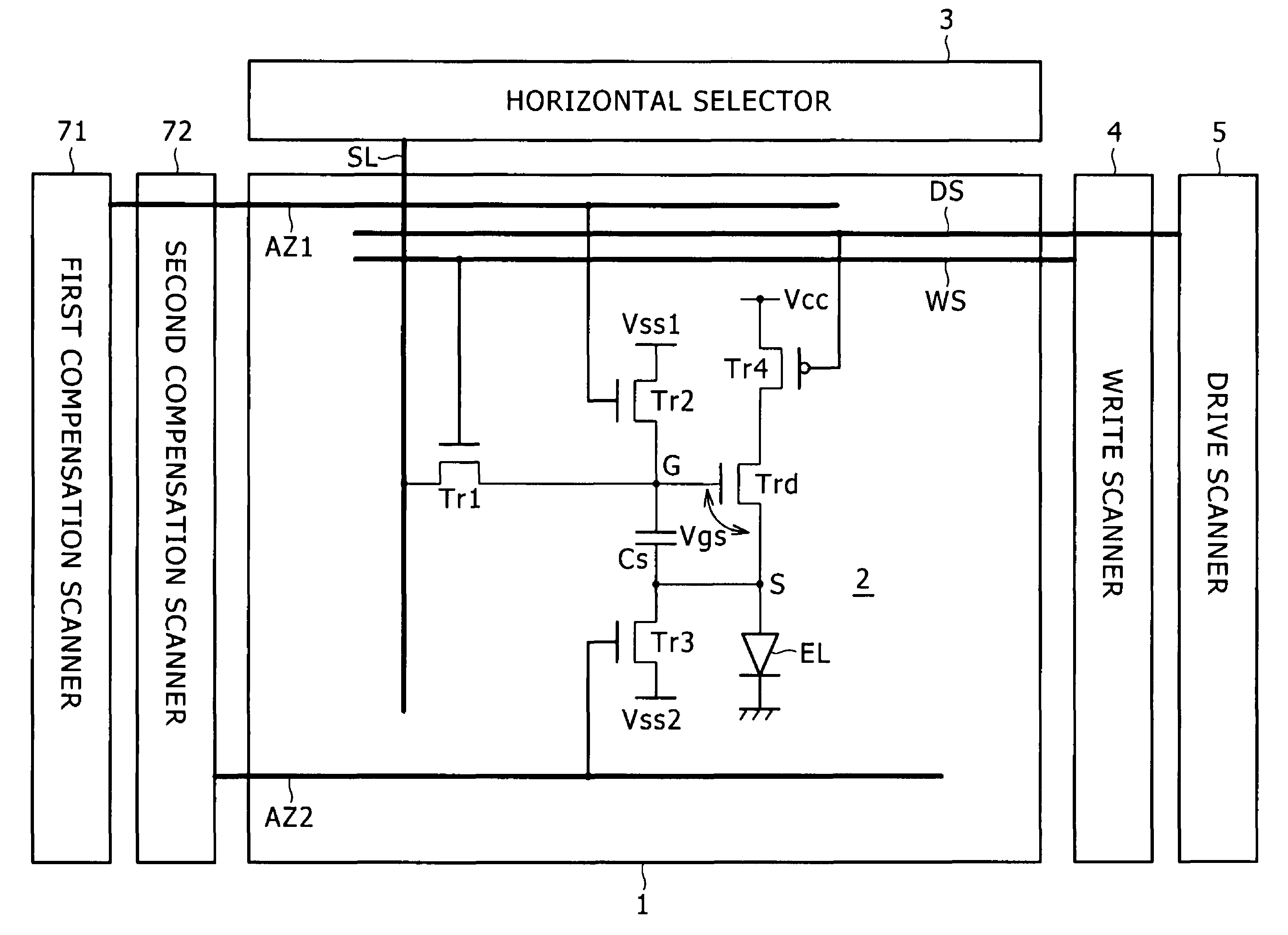
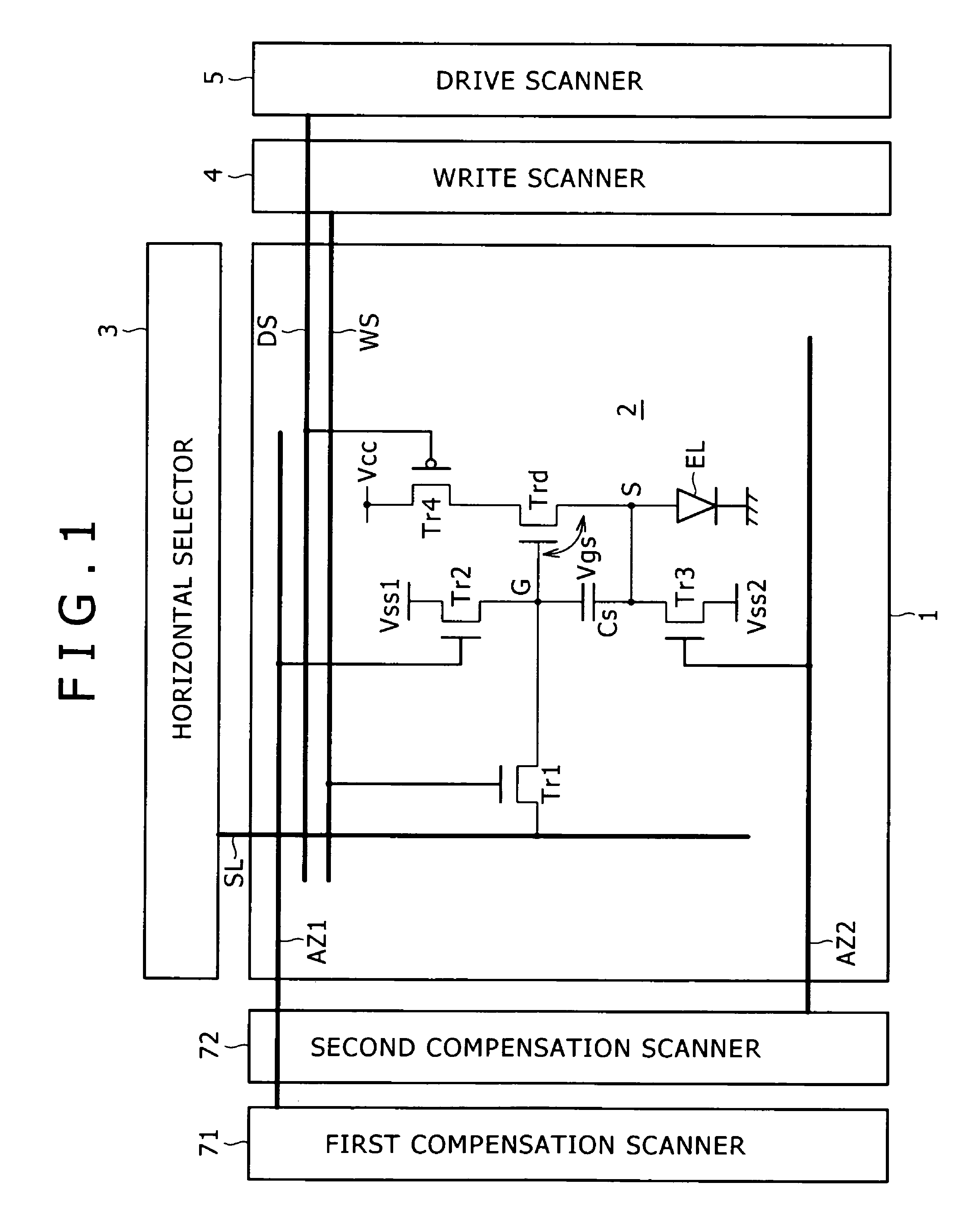
[0068]Preferred embodiments of the present invention are described in detail by referring to diagrams as follows. First of all, a typical reference implementation of an image display apparatus serving as the origin of the present invention is explained by referring to FIG. 1. As shown in the figure, the active-matrix image display apparatus includes a pixel-array unit 1 serving as the main unit and its peripheral circuits. The peripheral circuits include a horizontal selector 3, a write scanner 4, a drive scanner 5, a first compensation scanner 71 and a second compensation scanner 72. The pixel-array unit 1 has pixel circuits 2 laid out to form a matrix. Each of the pixel circuits 2 is placed at an intersection of a scanning line WS oriented in the row direction of the matrix and a data signal line SL oriented in the column direction of the matrix. In order to make the figure easy to understand, only one pixel circuit 2 is shown in an enlarged form. The horizontal selector 3 drives ...


PUM


Abstract

Disclosed herein is a display apparatus including a pixel-array unit, a scanner unit and a signal unit. The pixel-array unit has pixels laid out to form a matrix and each provided at an intersection of first and second scanning lines each oriented in a row direction of the matrix and a signal line oriented in a column direction of the matrix. The signal unit provides a video signal to the signal line. The scanner unit sequentially scans the pixels of the matrix in row units by supplying first and second control signals to the first and second scanning lines respectively.

Description

CROSS REFERENCES TO RELATED APPLICATIONS[0001]The present invention contains subject matter related to Japanese Patent Application JP 2005-328337, JP 2005-344207, and JP 2005-372621, filed in the Japanese Patent Office on Nov. 14, 2005, Nov. 29, 2005, and Dec. 26, 2005, respectively, the entire contents of which being incorporated herein by reference.BACKGROUND OF THE INVENTION[0002]1. Field of the Invention[0003]The present invention relates to a display apparatus for displaying an image by driving a current to flow to a light emitting device placed in each pixel. To put it in more detail, the present invention relates to an image display apparatus pertaining to the so-called active-matrix type category as a display apparatus employing an insulated-gate type field-effect transistor in every pixel as a transistor for controlling the magnitude of a current flowing through a light emitting device included in the pixel as a device typically made of an organic EL device.[0004]2. Descrip...

Claims


Application Information

Patent Timeline
Patent Type & Authority Patents(United States)
IPC IPC(8): G09G3/30H05B44/00
CPCG09G3/3233G09G2300/0819G09G2300/0842G09G2300/0861G09G2300/0866G09G2310/0205G09G2310/0251G09G2320/043
Inventor UCHINO, KATSUHIDEYAMASHITA, JUNICHIIZUMI, GAKUNAKAMURA, KAZUOYAMAMOTO, TETSURO
Owner SONY CORP
Why Eureka
Try Eureka