Method and apparatus for determining mask layouts for a multiple patterning process

a multiple patterning and mask technology, applied in the field of integrated circuit design and fabrication, can solve problems such as inability to manufacture technology, and achieve the effect of increasing the trenches and improving the process latitud

Active Publication Date: 2011-09-27
SYNOPSYS INC
View PDF6 Cites 13 Cited by
  • Summary
  • Abstract
  • Description
  • Claims
  • Application Information

AI Technical Summary

Benefits of technology

[0007]During operation, the system can receive a design intent. Next, the system can determine a set of critical edges which may need to be printed using different masks. The system can then determine a first trench and a second trench using a first edge and a second edge, respectively. Next, the system can assign the first trench and the second trench to a first mask and a second mask, respectively. The system can then increase the first trench and the second trench. Specifically, the system can keep increasing the trenches as long as they do not violate a design rule. The system can also adjust trench sizes to improve process latitude. One embodiment concurrently adjusts the sizes of the first trench and the second trench.

Problems solved by technology

Unfortunately, these technologies may not be ready for production in the near future.

Method used


Image

  • Method and apparatus for determining mask layouts for a multiple patterning process
  • Method and apparatus for determining mask layouts for a multiple patterning process
  • Method and apparatus for determining mask layouts for a multiple patterning process

Examples


Embodiment Construction

Integrated Circuit (IC) Design Flow

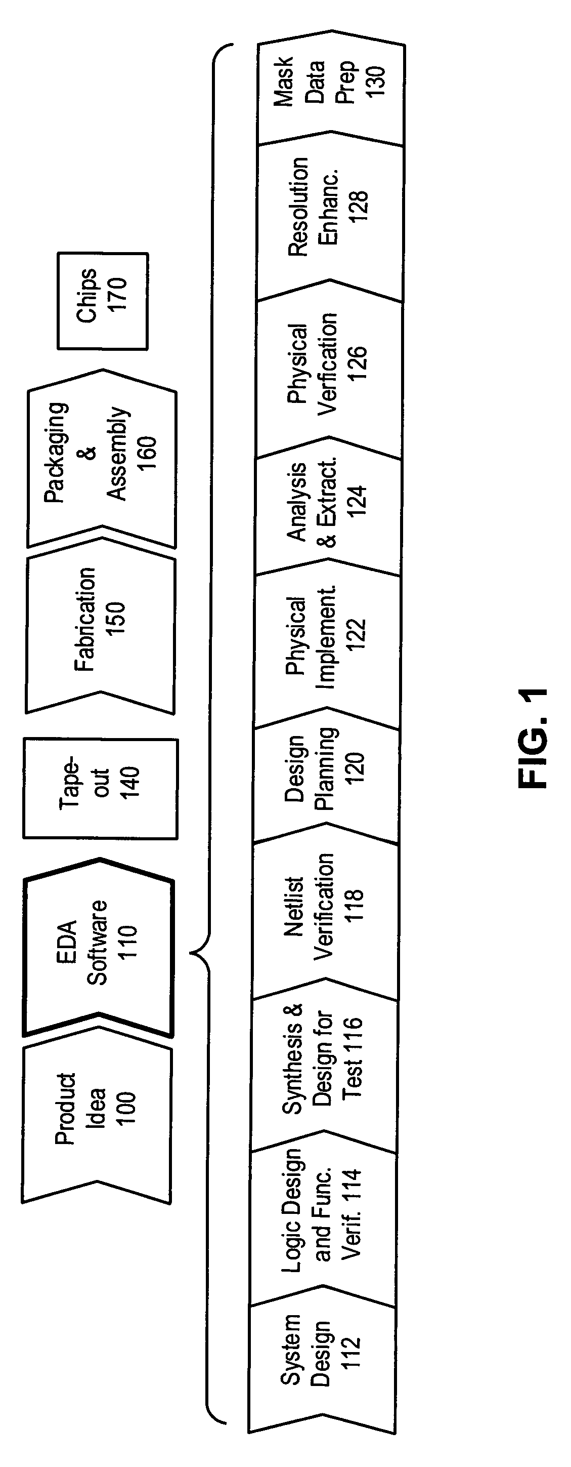
[0018]FIG. 1 illustrates various steps in the design and fabrication of an integrated circuit in accordance with an embodiment of the present invention.

[0019]The process starts with the conception of the product idea (step 100) which is realized using an EDA software design process (step 110). When the design is finalized, it can be taped-out (event 140). After tape out, the fabrication process (step 150) and packaging and assembly processes (step 160) are performed which ultimately result in finished chips (result 170).

[0020]The EDA software design process (step 110), in turn, comprises steps 112-130, which are described below. Note that the design flow description is for illustration purposes only. This description is not meant to limit the present invention. For example, an actual integrated circuit design may require the designer to perform the design steps in a different sequence than the sequence described below. The following discussion prov...


PUM


Abstract

One embodiment provides a method for determining mask layouts. During operation, the system can receive a design intent. Next, the system can determine a set of critical edges in the design layout, and select a first edge and a second edge. The system can then determine a first trench and a second trench using the first edge and the second edge, respectively. Note that an edge of the first trench may substantially overlap with the first edge, and an edge of the second trench may substantially overlap with the second edge. Next, the system may assign the first trench and the second trench to the first mask layout and the second mask layout, respectively. The system can then increase the first trench and the second trench, thereby improving pattern fidelity. The resulting mask layouts may be used in a double patterning process.

Description

BACKGROUND[0001]1. Field of the Invention[0002]The present invention relates to integrated circuit design and fabrication. More specifically, the present invention relates to a method and an apparatus to determine mask layouts for a multiple patterning process.[0003]2. Related Art[0004]Dramatic improvements in semiconductor integration densities have largely been achieved through corresponding improvements in semiconductor manufacturing technologies. As semiconductor manufacturing technologies move into the deep sub-micron era, the semiconductor industry is considering a number of new technologies, such as, extreme ultraviolet (EUV) lithography and immersion lithography. Unfortunately, these technologies may not be ready for production in the near future.[0005]Multiple patterning is a promising technology that can increase integration densities using today's process technologies. This technology uses multiple masks to realize features on a wafer. It is desirable to develop systems a...

Claims


Application Information

Patent Timeline
Patent Type & Authority Patents(United States)
IPC IPC(8): G06F17/50
CPCG03F1/144G03F1/70
Inventor DRAPEAU, MARTINMAYHEW, JEFFREY P.
Owner SYNOPSYS INC
Why Eureka
Try Eureka