SIC power DMOSFET with self-aligned source contact

a source contact and self-aligning technology, applied in the field of field-effect transistors with self-aligning source contacts, can solve problems such as its utilization beyond certain parameters

Active Publication Date: 2011-10-11
THE TRUSTEES OF PURDUE UNIV
View PDF29 Cites 57 Cited by
  • Summary
  • Abstract
  • Description
  • Claims
  • Application Information

AI Technical Summary

Benefits of technology

[0009]The present invention provides high voltage power MOSFETs, w

Problems solved by technology

Although silicon has been the material of choice for many semiconductor applications, its fundam

Method used


Image

  • SIC power DMOSFET with self-aligned source contact
  • SIC power DMOSFET with self-aligned source contact
  • SIC power DMOSFET with self-aligned source contact

Examples


Embodiment Construction

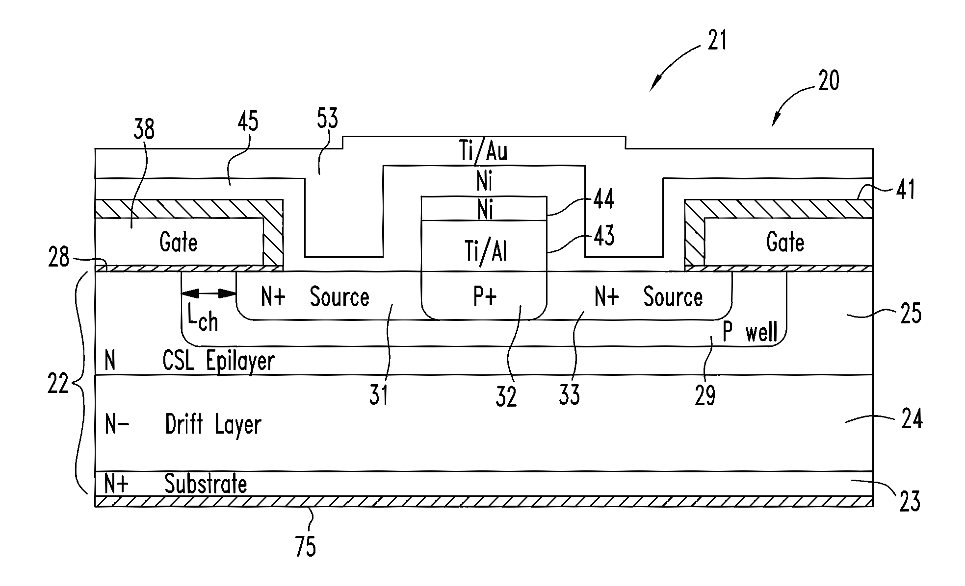
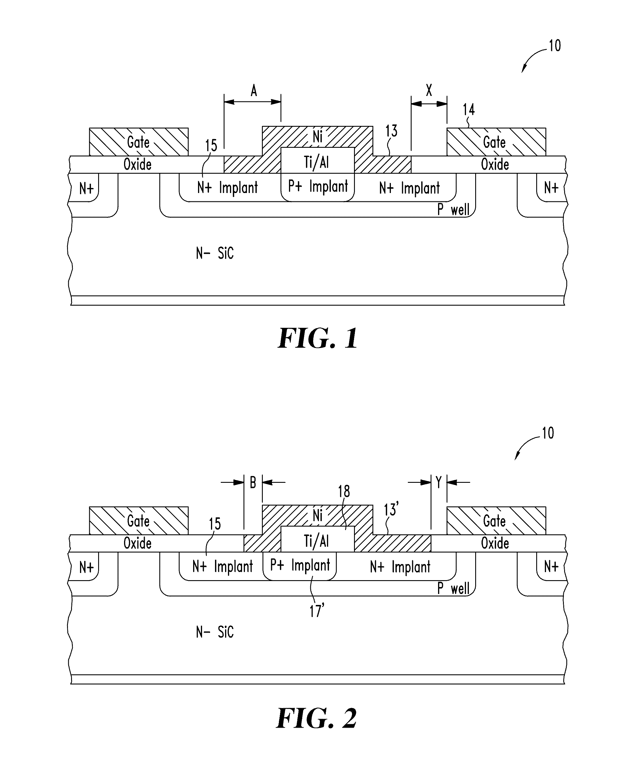
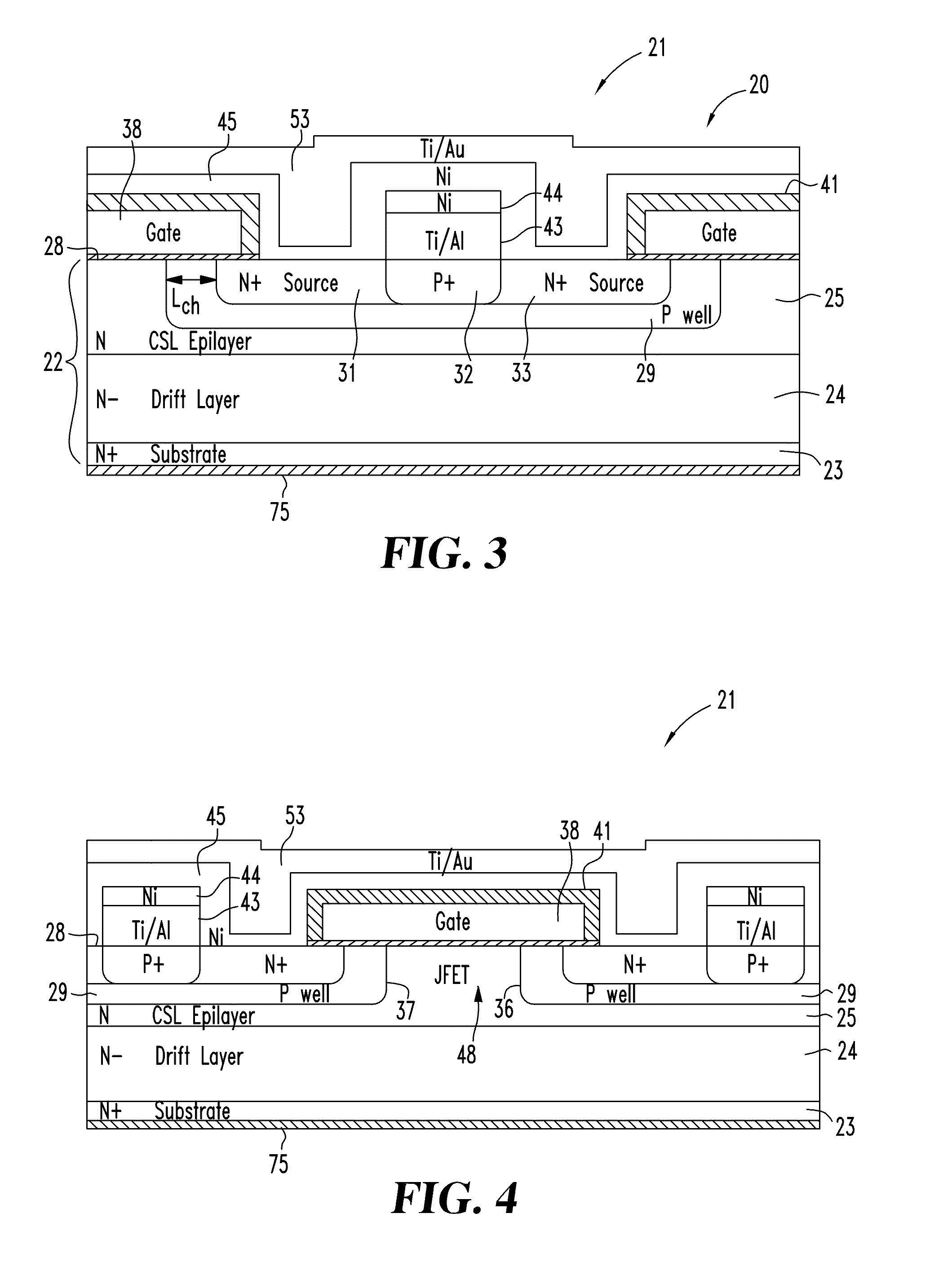
[0019]For the purpose of promoting an understanding of the principles of the invention, reference will now be made to the embodiments illustrated in the drawings and specific language will be used to describe the same. It will nevertheless be understood that no limitation of the scope of the invention is thereby intended, and that alterations and further modifications in the illustrated device and further applications of the principles of the invention as illustrated therein are contemplated as would normally occur to one skilled in the art to which the invention relates. As shown in the Figures, the sizes of some layers or regions are exaggerated to better illustrate the general structures of the present invention, and actual sizes—often with thicknesses of 50 nm—are either specified or are understood by persons of skill in the art to be other than that shown in the Figures.

[0020]It is desired in power DMOSFETs to have a low specific on-resistance (RON,SP), which is defined as the ...


PUM


Abstract

An intermediate product in the fabrication of a MOSFET, including a silicon carbide wafer having a substrate and a drift layer on said substrate, said drift layer having a plurality of source regions formed adjacent an upper surface thereof; a first oxide layer on said upper surface of said drift layer; a plurality of polysilicon gates above said first oxide layer, said plurality of polysilicon gates including a first gate adjacent a first of said source regions; an oxide layer over said first source region of greater thickness than said first oxide layer; and, an oxide layer over said first gate of substantially greater thickness than said oxide layer over said first source region.

Description

CROSS-REFERENCE TO RELATED APPLICATION[0001]This application claims the benefit of U.S. Provisional Patent Application Ser. No. 61 / 047,274, filed Apr. 23, 2008, which application is hereby incorporated by reference.GOVERNMENT RIGHTS[0002]This invention was made with government support under Contract / Grant No. W56HZV-06-C-0228 awarded by the U.S. Army TACOM LCMC, and Contract / Grant No. N00014-05-1-0437 awarded by DARPA. The government has certain rights in the invention.BACKGROUND OF THE INVENTION[0003]This invention relates generally to semiconductor field effect transistors, and more particularly to field effect transistors having self-aligned source contacts.[0004]The metal oxide semiconductor field effect transistor (MOSFET) is a device used to amplify or switch electronic signals. Power MOSFETs are well known for their ability to carry large currents in the on-state while withstanding large breakdown voltages in the off-state. In such devices, current flow between source and dra...

Claims


Application Information

Patent Timeline
IPC IPC(8): H01L31/0312
CPCH01L23/544H01L29/45H01L29/7802H01L29/66068H01L29/0878H01L29/41741H01L29/4238H01L2924/0002H01L2223/54426H01L2223/5446H01L2924/00
Inventor COOPER, JAMES A.SAHA, ASMITA
Owner THE TRUSTEES OF PURDUE UNIV
Why Eureka
Try Eureka